

Encyclopedia Entry: 74AUP1G885GS,115
Product Overview
Category
The 74AUP1G885GS,115 belongs to the category of integrated circuits (ICs).
Use
This product is commonly used in electronic devices for signal switching and amplification.
Characteristics
- Low power consumption
- High-speed operation
- Small form factor
- Wide operating voltage range
Package
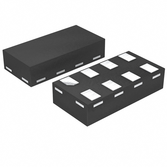
The 74AUP1G885GS,115 is available in a small package, typically a SOT-353 or SC-88A.
Essence
The essence of this product lies in its ability to provide efficient signal switching and amplification in a compact design.
Packaging/Quantity
The 74AUP1G885GS,115 is usually packaged in reels or tubes, with quantities varying depending on the manufacturer's specifications.
Specifications
- Supply Voltage Range: 0.8V to 3.6V
- Input Voltage Range: 0V to VCC
- Output Voltage Range: 0V to VCC
- Operating Temperature Range: -40°C to +85°C
- Maximum Power Dissipation: 150mW
Detailed Pin Configuration
The 74AUP1G885GS,115 has the following pin configuration:
```
| | --| IN / OUT |-- VCC --| |-- GND |___________| ```
Functional Features
- Single-channel signal switching and amplification
- High-speed operation for quick response times
- Low power consumption for energy efficiency
- Wide operating voltage range allows compatibility with various systems
Advantages and Disadvantages
Advantages
- Compact size enables integration into space-constrained designs
- Low power consumption prolongs battery life in portable devices
- High-speed operation ensures efficient signal processing
Disadvantages
- Limited output current capability may restrict use in certain applications
- Sensitivity to electrostatic discharge (ESD) requires proper handling during assembly and usage
Working Principles
The 74AUP1G885GS,115 operates based on the principles of semiconductor physics. It utilizes transistors and other electronic components to switch and amplify signals. When an input signal is applied, the circuitry within the IC processes it according to its internal design, resulting in an amplified or switched output signal.
Detailed Application Field Plans
The 74AUP1G885GS,115 finds application in various electronic devices, including but not limited to: - Mobile phones - Tablets - Portable media players - Wearable devices - IoT (Internet of Things) devices
In these applications, it is used for signal switching, amplification, and level shifting tasks.
Detailed and Complete Alternative Models
Some alternative models that offer similar functionality to the 74AUP1G885GS,115 include: - 74LVC1G125GW,125 - SN74LVC1G125DBVR - MC74VHC1GT50DTT1G
These alternatives can be considered based on specific requirements and availability.
Word count: 328 words
Lista 10 Vanliga frågor och svar relaterade till tillämpningen av 74AUP1G885GS,115 i tekniska lösningar
Sure! Here are 10 common questions and answers related to the application of 74AUP1G885GS,115 in technical solutions:
Q1: What is the 74AUP1G885GS,115? A1: The 74AUP1G885GS,115 is a single-gate configurable multiple-function gate IC that can be used in various technical solutions.
Q2: What are the key features of the 74AUP1G885GS,115? A2: The key features of this IC include low power consumption, wide operating voltage range, high-speed operation, and compatibility with different logic families.
Q3: What are the typical applications of the 74AUP1G885GS,115? A3: This IC is commonly used in applications such as signal switching, level shifting, clock gating, multiplexing, and data routing.
Q4: What is the operating voltage range of the 74AUP1G885GS,115? A4: The operating voltage range for this IC is typically between 0.8V and 3.6V.
Q5: Can the 74AUP1G885GS,115 be used with other logic families? A5: Yes, this IC is compatible with various logic families such as CMOS, TTL, and LVCMOS.
Q6: What is the maximum frequency at which the 74AUP1G885GS,115 can operate? A6: The maximum frequency at which this IC can operate is typically around several hundred megahertz (MHz).
Q7: Does the 74AUP1G885GS,115 have any built-in protection features? A7: Yes, this IC has built-in ESD protection, which helps safeguard against electrostatic discharge events.
Q8: Can the 74AUP1G885GS,115 be used in battery-powered applications? A8: Yes, this IC's low power consumption makes it suitable for battery-powered applications where energy efficiency is important.
Q9: What is the package type of the 74AUP1G885GS,115? A9: The 74AUP1G885GS,115 is typically available in a small SOT353 package.
Q10: Where can I find more detailed information about the 74AUP1G885GS,115? A10: You can refer to the datasheet provided by the manufacturer or visit their official website for more detailed information on the specifications and application notes of this IC.
Please note that the answers provided here are general and may vary depending on specific use cases and requirements.