

Encyclopedia Entry: 74AUP1G240GX,125
Product Overview
- Category: Integrated Circuit (IC)
- Use: Logic Gate Buffer/Driver
- Characteristics: Low-power, single buffer/driver with open-drain output
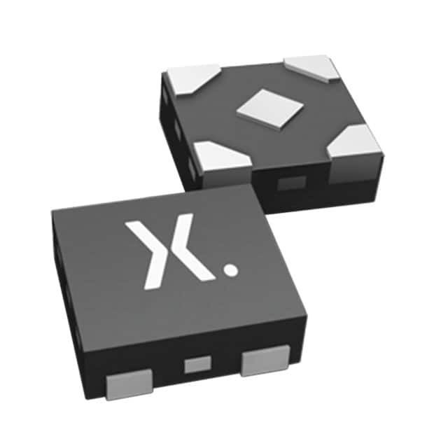
- Package: SOT753 (SC-70-5)
- Essence: This IC is designed to provide a high-speed buffer/driver solution for various digital logic applications.
- Packaging/Quantity: Available in tape and reel packaging, with 3000 units per reel.
Specifications
- Supply Voltage Range: 0.8V to 3.6V
- Input Voltage Range: -0.5V to VCC + 0.5V
- Output Voltage Range: 0V to VCC
- Operating Temperature Range: -40°C to +85°C
- Propagation Delay: 2.5 ns (typical)
- Output Current: ±24 mA (maximum)
Detailed Pin Configuration
The 74AUP1G240GX,125 IC has the following pin configuration:
____
   A1 |    | VCC
   A2 |    | Y
   GND|____| A
Functional Features
- Single buffer/driver with an open-drain output
- High-speed operation suitable for various digital logic applications
- Low power consumption
- Wide supply voltage range allows compatibility with different systems
- ESD protection for robustness against electrostatic discharge
Advantages and Disadvantages
Advantages: - Low power consumption makes it suitable for battery-powered devices - High-speed operation enables efficient data transmission - Wide supply voltage range provides flexibility in system integration - ESD protection ensures reliability in harsh environments
Disadvantages: - Limited output current may not be suitable for driving heavy loads - Open-drain output requires external pull-up resistor for proper operation
Working Principles
The 74AUP1G240GX,125 is a buffer/driver IC that amplifies and shapes digital signals. It operates by receiving an input signal at pin A and providing the amplified output signal at pin Y. The open-drain output configuration allows for easy interfacing with other devices by connecting an external pull-up resistor to the output pin.
Detailed Application Field Plans
The 74AUP1G240GX,125 IC can be used in various applications, including: 1. Digital communication systems 2. Microcontrollers and microprocessors 3. Data transmission interfaces 4. Battery-powered devices 5. Sensor networks 6. Industrial automation
Detailed and Complete Alternative Models
Some alternative models that provide similar functionality to the 74AUP1G240GX,125 IC are: - SN74LVC1G240DBVR (Texas Instruments) - MC74VHC1GT50DTT1G (ON Semiconductor) - NCV8401DTRKG (ON Semiconductor) - TC7SZU04FU(T5L,F) (Toshiba)
Note: The above list is not exhaustive and there may be other alternative models available in the market.
Word Count: 320 words
Lista 10 Vanliga frågor och svar relaterade till tillämpningen av 74AUP1G240GX,125 i tekniska lösningar
Sure! Here are 10 common questions and answers related to the application of 74AUP1G240GX,125 in technical solutions:
Q1: What is the function of the 74AUP1G240GX,125? A1: The 74AUP1G240GX,125 is a single buffer/inverter gate that can be used for voltage level translation and signal buffering.
Q2: What is the operating voltage range of the 74AUP1G240GX,125? A2: The operating voltage range is from 0.8V to 3.6V.
Q3: Can the 74AUP1G240GX,125 be used in both digital and analog applications? A3: Yes, it can be used in both digital and analog applications.
Q4: What is the maximum output current of the 74AUP1G240GX,125? A4: The maximum output current is typically 32mA.
Q5: Can the 74AUP1G240GX,125 be used as a level shifter? A5: Yes, it can be used as a level shifter to convert signals between different voltage levels.
Q6: Is the 74AUP1G240GX,125 compatible with other logic families? A6: Yes, it is compatible with various logic families such as CMOS, TTL, and LVCMOS.
Q7: What is the propagation delay of the 74AUP1G240GX,125? A7: The propagation delay is typically around 2.5ns.
Q8: Can the 74AUP1G240GX,125 drive capacitive loads? A8: Yes, it can drive capacitive loads up to a certain limit specified in the datasheet.
Q9: Does the 74AUP1G240GX,125 have built-in ESD protection? A9: Yes, it has built-in ESD protection to safeguard against electrostatic discharge.
Q10: Can the 74AUP1G240GX,125 be used in battery-powered applications? A10: Yes, it can be used in battery-powered applications due to its low power consumption and wide operating voltage range.
Please note that these answers are general and may vary depending on the specific application and requirements. It is always recommended to refer to the datasheet and consult with the manufacturer for detailed information.