

Encyclopedia Entry: 74AUP1G07GX,125
Product Overview
- Category: Integrated Circuit (IC)
- Use: Logic Gate Buffer/Driver
- Characteristics: Low-power, single buffer/driver with open-drain output
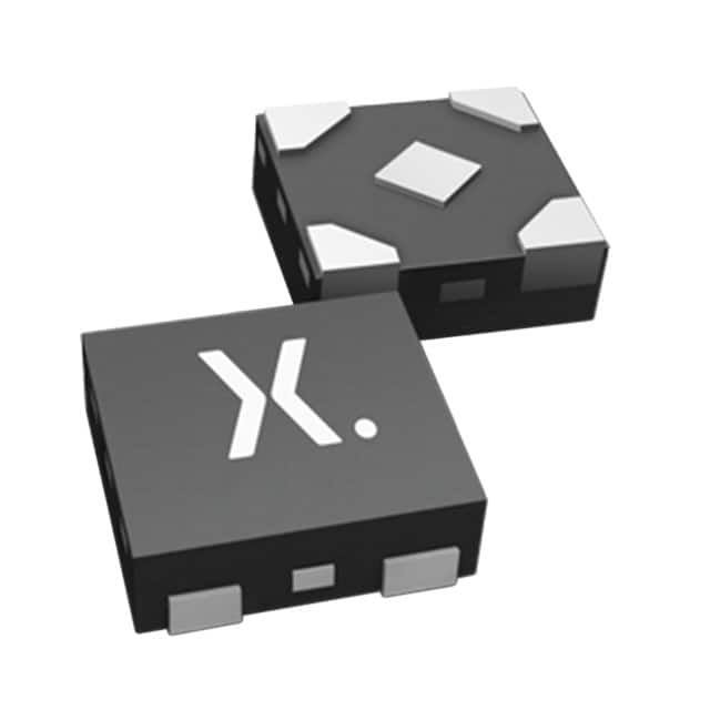
- Package: SOT353 (SC-88A), 5-pin package
- Essence: Provides voltage level shifting and signal buffering capabilities
- Packaging/Quantity: Tape and Reel, 3000 pieces per reel
Specifications
- Supply Voltage Range: 0.8V to 3.6V
- Input Voltage Range: -0.5V to VCC + 0.5V
- Output Voltage Range: 0V to VCC
- Maximum Output Current: ±32mA
- Propagation Delay: 2.7ns (typical)
- Operating Temperature Range: -40°C to +85°C
Detailed Pin Configuration
The 74AUP1G07GX,125 IC has the following pin configuration:
____
   1 |o    |
   2 |     |
   3 |     |
   4 |     |
   5 |____o|
Pin Description: 1. GND: Ground 2. IN: Input Signal 3. NC: No Connection 4. OE: Output Enable 5. OUT: Buffered Output Signal
Functional Features
- Single buffer/driver with open-drain output
- Provides voltage level shifting between different logic levels
- Can be used as a buffer to increase the driving capability of a weak signal
- Supports bidirectional communication between devices with different voltage levels
- Low power consumption makes it suitable for battery-powered applications
Advantages
- Wide supply voltage range allows compatibility with various systems
- Small package size saves board space in compact designs
- Open-drain output allows easy interfacing with other devices
- Low propagation delay ensures fast signal transmission
Disadvantages
- Limited output current may not be suitable for high-power applications
- No internal pull-up resistor, requiring an external resistor for proper operation in some cases
Working Principles
The 74AUP1G07GX,125 is a single buffer/driver IC that operates as a voltage level shifter and signal buffer. It takes an input signal and provides a buffered output signal with an open-drain configuration. The device can shift the logic levels of signals between different voltage domains, allowing communication between devices operating at different voltage levels.
Detailed Application Field Plans
The 74AUP1G07GX,125 is commonly used in various applications, including: 1. Battery-powered devices: Due to its low power consumption, it is suitable for portable electronics such as smartphones, tablets, and wearables. 2. Industrial automation: It can be used in control systems, sensors, and actuators that require voltage level shifting and signal buffering. 3. Communication systems: The IC facilitates bidirectional communication between devices operating at different voltage levels, making it useful in networking equipment and interface circuits.
Alternative Models
Other alternative models that provide similar functionality to the 74AUP1G07GX,125 include: - SN74LVC1G07DBVR (Texas Instruments) - MC74VHC1GT07DF1G (ON Semiconductor) - NC7SZ07P5X (Fairchild Semiconductor)
Note: These alternative models may have slight differences in specifications and pin configurations.
Lista 10 Vanliga frågor och svar relaterade till tillämpningen av 74AUP1G07GX,125 i tekniska lösningar
Sure! Here are 10 common questions and answers related to the application of 74AUP1G07GX,125 in technical solutions:
Q1: What is the function of the 74AUP1G07GX,125? A1: The 74AUP1G07GX,125 is a single buffer/driver with open-drain output that can be used for level shifting or signal buffering in various applications.
Q2: What is the operating voltage range of the 74AUP1G07GX,125? A2: The 74AUP1G07GX,125 operates within a voltage range of 0.8V to 3.6V.
Q3: Can the 74AUP1G07GX,125 handle high-speed signals? A3: Yes, the 74AUP1G07GX,125 is designed to handle high-speed signals with a maximum propagation delay of 2.5 ns.
Q4: How many inputs does the 74AUP1G07GX,125 have? A4: The 74AUP1G07GX,125 has one input.
Q5: What is the maximum output current of the 74AUP1G07GX,125? A5: The 74AUP1G07GX,125 can sink up to 32 mA of current.
Q6: Can the 74AUP1G07GX,125 be used as a level shifter? A6: Yes, the 74AUP1G07GX,125 can be used as a level shifter to convert signals between different voltage levels.
Q7: Is the 74AUP1G07GX,125 compatible with other logic families? A7: Yes, the 74AUP1G07GX,125 is compatible with a wide range of logic families, including CMOS, TTL, and LVCMOS.
Q8: What is the package type of the 74AUP1G07GX,125? A8: The 74AUP1G07GX,125 is available in a small SOT353 package.
Q9: Can the 74AUP1G07GX,125 be used in battery-powered applications? A9: Yes, the 74AUP1G07GX,125 is suitable for battery-powered applications due to its low power consumption.
Q10: Are there any recommended applications for the 74AUP1G07GX,125? A10: The 74AUP1G07GX,125 can be used in various applications such as level shifting, signal buffering, I2C bus interface, and general-purpose logic-level conversion.
Please note that these answers are based on general information about the 74AUP1G07GX,125. For specific details and application requirements, it is always recommended to refer to the datasheet or consult the manufacturer's documentation.