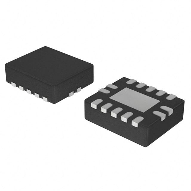
74AHCT126BQ-Q100,1
Basic Information Overview
- Category: Integrated Circuit (IC)
- Use: Logic Gate Buffer/Driver
- Characteristics: High-speed, low-power, compatible with TTL and CMOS logic levels
- Package: SOIC (Small Outline Integrated Circuit)
- Essence: Quad buffer/driver with 3-state outputs
- Packaging/Quantity: Tape and Reel, 2500 units per reel
Specifications
- Supply Voltage Range: 4.5V to 5.5V
- Input Voltage Range: 0V to VCC
- Output Voltage Range: 0V to VCC
- Operating Temperature Range: -40°C to +125°C
- Output Current: ±8mA
- Propagation Delay: 6ns (typical)
Detailed Pin Configuration
The 74AHCT126BQ-Q100,1 IC has a total of 14 pins, which are assigned as follows:
- 1A (Input 1)
- 1Y (Output 1)
- 2A (Input 2)
- 2Y (Output 2)
- 3A (Input 3)
- 3Y (Output 3)
- 4A (Input 4)
- 4Y (Output 4)
- GND (Ground)
- 1OE (Output Enable Input)
- 2OE (Output Enable Input)
- 3OE (Output Enable Input)
- 4OE (Output Enable Input)
- VCC (Supply Voltage)
Functional Features
- Quad buffer/driver with 3-state outputs
- Non-inverting buffer/driver function
- Outputs can be disabled using the output enable inputs (1OE, 2OE, 3OE, 4OE)
- High-speed operation with low power consumption
- Compatible with both TTL and CMOS logic levels
- Provides improved noise immunity
Advantages and Disadvantages
Advantages: - High-speed operation allows for efficient data transmission - Low-power consumption helps in reducing energy usage - Compatibility with TTL and CMOS logic levels enables easy integration into existing systems - Improved noise immunity ensures reliable signal transmission
Disadvantages: - Limited output current may restrict its use in certain applications requiring higher current capabilities - The operating temperature range may not be suitable for extreme environments
Working Principles
The 74AHCT126BQ-Q100,1 is a quad buffer/driver IC that amplifies and buffers digital signals. It operates by receiving input signals (1A, 2A, 3A, 4A) and providing corresponding amplified outputs (1Y, 2Y, 3Y, 4Y). The output enable inputs (1OE, 2OE, 3OE, 4OE) control the state of the outputs, allowing them to be enabled or disabled.
Detailed Application Field Plans
The 74AHCT126BQ-Q100,1 IC finds applications in various fields, including: 1. Communication Systems: Used for signal buffering and driving in data communication networks. 2. Industrial Automation: Enables signal amplification and level shifting in control systems. 3. Automotive Electronics: Suitable for automotive applications requiring high-speed data transmission. 4. Consumer Electronics: Used in devices such as smartphones, tablets, and gaming consoles for signal conditioning and amplification.
Detailed and Complete Alternative Models
Some alternative models that can be considered as alternatives to the 74AHCT126BQ-Q100,1 IC are: - SN74AHCT126-Q1 - MC74AHCT126A - CD74HCT126E - 74HC126
These alternative models offer similar functionality and can be used as substitutes depending on specific requirements.
Word count: 410 words
Lista 10 Vanliga frågor och svar relaterade till tillämpningen av 74AHCT126BQ-Q100,1 i tekniska lösningar
Sure! Here are 10 common questions and answers related to the application of 74AHCT126BQ-Q100,1 in technical solutions:
1. What is the purpose of the 74AHCT126BQ-Q100,1? The 74AHCT126BQ-Q100,1 is a quad buffer/line driver IC that can be used to amplify or buffer digital signals.
2. What is the voltage range supported by the 74AHCT126BQ-Q100,1? The 74AHCT126BQ-Q100,1 supports a voltage range of 4.5V to 5.5V.
3. How many buffers/line drivers are there in the 74AHCT126BQ-Q100,1? The 74AHCT126BQ-Q100,1 has four independent buffers/line drivers.
4. What is the maximum output current of each buffer/line driver? Each buffer/line driver in the 74AHCT126BQ-Q100,1 can provide a maximum output current of 8mA.
5. Can the 74AHCT126BQ-Q100,1 be used for level shifting? Yes, the 74AHCT126BQ-Q100,1 can be used for level shifting as it supports both TTL and CMOS logic levels.
6. What is the propagation delay of the 74AHCT126BQ-Q100,1? The propagation delay of the 74AHCT126BQ-Q100,1 is typically 7.5ns.
7. Is the 74AHCT126BQ-Q100,1 suitable for high-speed applications? Yes, the 74AHCT126BQ-Q100,1 is designed for high-speed operation and can be used in applications with fast switching requirements.
8. Can the 74AHCT126BQ-Q100,1 be used in automotive applications? Yes, the 74AHCT126BQ-Q100,1 is qualified for automotive applications and meets the AEC-Q100 standard.
9. What is the package type of the 74AHCT126BQ-Q100,1? The 74AHCT126BQ-Q100,1 is available in a standard SOIC-14 package.
10. Are there any special considerations when using the 74AHCT126BQ-Q100,1? It is important to ensure proper decoupling and power supply bypassing for stable operation. Additionally, care should be taken to avoid exceeding the maximum ratings specified in the datasheet.
Please note that these answers are general and may vary depending on the specific application and requirements. It is always recommended to refer to the datasheet and consult the manufacturer for detailed information.


