

Encyclopedia Entry: 74AHC1G08GV,125
Product Overview
Category
The 74AHC1G08GV,125 belongs to the category of integrated circuits (ICs) and specifically falls under the logic gates subcategory.
Use
This product is primarily used for logical operations in digital circuits. It serves as a single 2-input AND gate, enabling the implementation of various logical functions.
Characteristics
- Low power consumption
- High-speed operation
- Wide supply voltage range
- Schmitt-trigger input for noise immunity
- Compatible with both CMOS and TTL voltage levels
Package
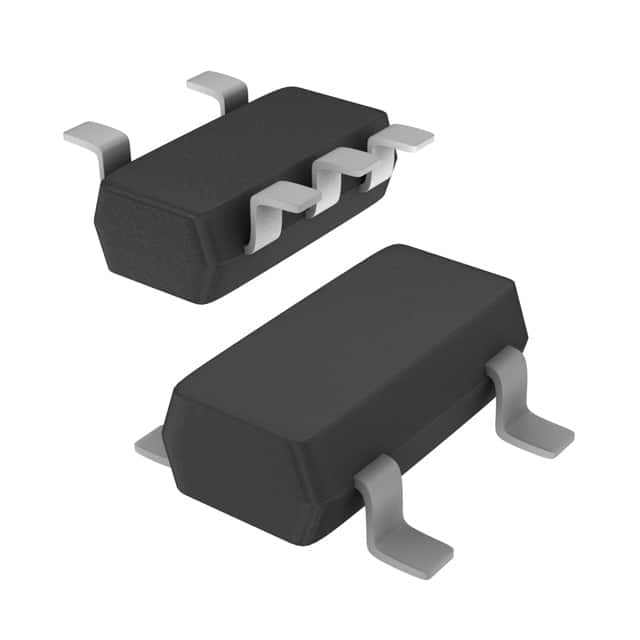
The 74AHC1G08GV,125 is available in a small SOT353 package, which ensures space-saving integration into electronic devices.
Essence
The essence of this product lies in its ability to perform logical AND operations efficiently and reliably within digital circuits.
Packaging/Quantity
The 74AHC1G08GV,125 is typically packaged in reels, containing a quantity of 3000 units per reel.
Specifications
- Supply Voltage Range: 2 V to 5.5 V
- Input Voltage Range: 0 V to VCC
- Output Voltage Range: 0 V to VCC
- Operating Temperature Range: -40°C to +125°C
- Propagation Delay: 4 ns (max)
- Quiescent Current: 1 µA (max)
Detailed Pin Configuration
The 74AHC1G08GV,125 has the following pin configuration:
+---+
   A --|   |-- VCC
   B --|   |-- Y
 GND --|   |--
       +---+
Functional Features
- Single 2-input AND gate functionality
- High-speed operation allows for efficient processing of logical operations
- Wide supply voltage range enables compatibility with various systems
- Schmitt-trigger input provides noise immunity, ensuring reliable operation in noisy environments
- Low power consumption makes it suitable for battery-powered devices
Advantages and Disadvantages
Advantages
- Compact size allows for space-saving integration into electronic devices
- Compatibility with both CMOS and TTL voltage levels enhances versatility
- Wide supply voltage range enables usage in a variety of applications
- High-speed operation ensures efficient processing of logical operations
Disadvantages
- Limited to 2-input AND gate functionality, limiting its application scope to specific logic operations
- May not be suitable for complex digital circuits requiring multiple logic gates
Working Principles
The 74AHC1G08GV,125 operates based on the principles of Boolean logic. It takes two input signals, A and B, and performs a logical AND operation on them. The output, Y, reflects the result of this operation. When both inputs are high (logic level 1), the output is also high. Otherwise, the output remains low (logic level 0).
Detailed Application Field Plans
The 74AHC1G08GV,125 finds applications in various fields, including:
- Digital electronics: Used in the design and implementation of digital circuits, such as microcontrollers, CPUs, and memory units.
- Communication systems: Employed in signal processing and data transmission circuits to perform logical operations on incoming signals.
- Industrial automation: Integrated into control systems to enable logical decision-making processes.
- Automotive electronics: Utilized in vehicle control units for performing logical operations related to safety systems, engine management, and more.
Detailed and Complete Alternative Models
Some alternative models that offer similar functionality to the 74AHC1G08GV,125 include:
- 74HC08: A widely used 2-input AND gate IC with comparable characteristics and pin configuration.
- SN74LVC1G08: Another 2-input AND gate IC with low voltage operation and similar performance specifications.
- CD4081: A quad 2-input AND gate IC that provides multiple AND gate functionality in a single package.
These alternative models can be considered based on specific requirements and compatibility with existing systems.
Word count: 511 words
Lista 10 Vanliga frågor och svar relaterade till tillämpningen av 74AHC1G08GV,125 i tekniska lösningar
Sure! Here are 10 common questions and answers related to the application of 74AHC1G08GV,125 in technical solutions:
Q1: What is the function of the 74AHC1G08GV,125? A1: The 74AHC1G08GV,125 is a single 2-input AND gate that performs logical AND operation on two input signals.
Q2: What is the operating voltage range for the 74AHC1G08GV,125? A2: The operating voltage range for the 74AHC1G08GV,125 is typically between 2.0V and 5.5V.
Q3: What is the maximum output current of the 74AHC1G08GV,125? A3: The maximum output current of the 74AHC1G08GV,125 is 8mA.
Q4: Can the 74AHC1G08GV,125 be used in both digital and analog applications? A4: No, the 74AHC1G08GV,125 is specifically designed for digital applications.
Q5: What is the propagation delay of the 74AHC1G08GV,125? A5: The propagation delay of the 74AHC1G08GV,125 is typically around 6 ns.
Q6: Can the 74AHC1G08GV,125 be used in high-speed applications? A6: Yes, the 74AHC1G08GV,125 is suitable for high-speed applications due to its low propagation delay.
Q7: Is the 74AHC1G08GV,125 compatible with other logic families? A7: Yes, the 74AHC1G08GV,125 is compatible with other CMOS logic families.
Q8: Can the 74AHC1G08GV,125 be used in battery-powered applications? A8: Yes, the 74AHC1G08GV,125 is suitable for battery-powered applications due to its low power consumption.
Q9: What is the package type of the 74AHC1G08GV,125? A9: The 74AHC1G08GV,125 is available in a SOT353 package.
Q10: Can the 74AHC1G08GV,125 be used in automotive applications? A10: Yes, the 74AHC1G08GV,125 is qualified for automotive applications and meets the necessary standards.
Please note that these answers are general and may vary depending on specific datasheet information or application requirements.