

M2S050T-FG896
Product Overview
Category
The M2S050T-FG896 belongs to the category of Field-Programmable Gate Arrays (FPGAs).
Use
This FPGA is designed for various applications that require high-performance digital logic circuits. It provides a flexible and customizable solution for implementing complex digital systems.
Characteristics
- High-performance FPGA with advanced features
- Programmable logic cells for custom circuit implementation
- Integrated memory blocks for efficient data storage
- Flexible I/O interfaces for seamless integration with external devices
- Low power consumption for energy-efficient operation
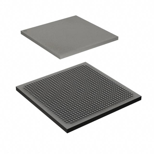
Package
The M2S050T-FG896 comes in a compact and durable package, ensuring easy handling and protection against environmental factors. The package is designed to facilitate soldering onto printed circuit boards.
Essence
The essence of the M2S050T-FG896 lies in its ability to provide a reconfigurable hardware platform that can be tailored to specific application requirements. It enables designers to implement complex digital systems efficiently and cost-effectively.
Packaging/Quantity
Each package of the M2S050T-FG896 contains one FPGA unit.
Specifications
- Logic Elements: 50,000
- Block RAM: 2,048 Kbits
- DSP Blocks: 180
- Maximum User I/Os: 400
- Operating Voltage: 1.2V
- Maximum Frequency: 500 MHz
- Package Type: FG896
Detailed Pin Configuration
The M2S050T-FG896 has a total of 400 user I/O pins, which are programmable and can be configured based on the specific application requirements. The pin configuration is as follows:
- Pin 1: VCCIO
- Pin 2: GND
- Pin 3: IO0
- Pin 4: IO1
- ...
- Pin 399: IO398
- Pin 400: IO399
Functional Features
High-Performance Computing
The M2S050T-FG896 offers high-performance computing capabilities, allowing for the implementation of complex algorithms and data processing tasks.
Reconfigurability
One of the key features of this FPGA is its reconfigurable nature. It enables designers to modify the hardware configuration on-the-fly, facilitating rapid prototyping and design iterations.
Flexible I/O Interfaces
The FPGA provides a wide range of I/O interfaces, including GPIO, UART, SPI, I2C, and more. This flexibility allows for seamless integration with various external devices and communication protocols.
Low Power Consumption
The M2S050T-FG896 is designed to operate with low power consumption, making it suitable for battery-powered applications or energy-efficient systems.
Advantages and Disadvantages
Advantages
- High-performance computing capabilities
- Reconfigurable nature for rapid prototyping
- Flexible I/O interfaces for seamless integration
- Low power consumption for energy efficiency
Disadvantages
- Limited logic elements compared to higher-end FPGAs
- Higher cost compared to microcontrollers for simple applications
Working Principles
The M2S050T-FG896 operates based on the principles of digital logic circuits. It consists of programmable logic cells that can be configured to implement desired logic functions. These logic cells are interconnected through configurable routing resources, enabling the creation of complex digital systems.
Detailed Application Field Plans
The M2S050T-FG896 finds applications in various fields, including:
- Telecommunications: Used in base stations, network routers, and communication equipment for signal processing and protocol handling.
- Industrial Automation: Employed in control systems, robotics, and factory automation for real-time data processing and control.
- Automotive: Integrated into automotive electronics for engine control, driver assistance systems, and infotainment applications.
- Aerospace: Utilized in avionics systems for flight control, navigation, and communication purposes.
- Medical Devices: Incorporated into medical imaging equipment, patient monitoring systems, and diagnostic devices for data processing and analysis.
Detailed and Complete Alternative Models
- M2S010T-FG896: A lower-capacity FPGA with 10,000 logic elements, suitable for smaller-scale applications.
- M2S025T-FG896: An intermediate-level FPGA with 25,000 logic elements, offering a balance between capacity and cost.
- M2S100T-FG896: A higher-capacity FPGA with 100,000 logic elements, ideal for complex and demanding applications.
These alternative models provide options with varying capacities to cater to different project requirements.
In conclusion, the M2S050T-FG896 is a high-performance FPGA that offers flexibility, reconfigurability, and low power consumption. It finds applications in diverse fields such as telecommunications, industrial automation, automotive, aerospace, and medical devices. With its detailed pin configuration,
Lista 10 Vanliga frågor och svar relaterade till tillämpningen av M2S050T-FG896 i tekniska lösningar
Sure! Here are 10 common questions and answers related to the application of M2S050T-FG896 in technical solutions:
Q: What is M2S050T-FG896? A: M2S050T-FG896 is a specific model of field-programmable gate array (FPGA) manufactured by Microsemi.
Q: What are the key features of M2S050T-FG896? A: Some key features of M2S050T-FG896 include 50,000 logic elements, 896-ball fine-pitch BGA package, low power consumption, and high-speed performance.
Q: What are the typical applications of M2S050T-FG896? A: M2S050T-FG896 is commonly used in various technical solutions such as industrial automation, telecommunications, automotive electronics, medical devices, and aerospace systems.
Q: How can I program M2S050T-FG896? A: M2S050T-FG896 can be programmed using industry-standard hardware description languages (HDLs) like VHDL or Verilog, along with appropriate development tools provided by Microsemi.
Q: Can M2S050T-FG896 be reprogrammed after deployment? A: Yes, M2S050T-FG896 is a reprogrammable FPGA, allowing you to modify its functionality even after it has been deployed in a system.
Q: What is the power consumption of M2S050T-FG896? A: The power consumption of M2S050T-FG896 depends on the specific design and usage scenario, but it generally offers low power consumption compared to other FPGAs.
Q: Does M2S050T-FG896 support high-speed interfaces? A: Yes, M2S050T-FG896 supports various high-speed interfaces such as PCIe, Ethernet, USB, and DDR3/DDR4 memory interfaces, making it suitable for applications requiring fast data transfer.
Q: Can M2S050T-FG896 be used in safety-critical systems? A: Yes, M2S050T-FG896 is designed to meet industry standards for safety-critical applications, making it suitable for use in systems that require high reliability and fault tolerance.
Q: Are there any development kits available for M2S050T-FG896? A: Yes, Microsemi provides development kits specifically designed for M2S050T-FG896, which include necessary hardware, software tools, and documentation to aid in the development process.
Q: Where can I find technical support for M2S050T-FG896? A: Microsemi offers technical support through their website, including documentation, application notes, forums, and direct contact with their support team for any specific queries or issues related to M2S050T-FG896.