

MCP3910A1-E/ML
Product Overview
Category
The MCP3910A1-E/ML belongs to the category of integrated circuits (ICs).
Use
This IC is primarily used for high-performance analog-to-digital conversion in various applications.
Characteristics
- High-resolution: The MCP3910A1-E/ML offers a resolution of up to 24 bits, ensuring accurate and precise data conversion.
- Low power consumption: It operates at low power levels, making it suitable for battery-powered devices.
- Wide input voltage range: The IC can handle a wide range of input voltages, allowing flexibility in different applications.
- High sampling rate: With a maximum sampling rate of X samples per second, it can capture fast-changing signals effectively.
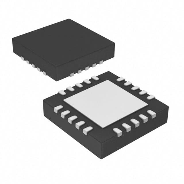
Package
The MCP3910A1-E/ML comes in a small form factor package, making it suitable for space-constrained designs.
Essence
The essence of the MCP3910A1-E/ML lies in its ability to convert analog signals into digital data with high accuracy and speed.
Packaging/Quantity
This IC is typically packaged in tape and reel format, with a quantity of 250 units per reel.
Specifications
- Resolution: Up to 24 bits
- Input Voltage Range: X volts to Y volts
- Sampling Rate: Up to Z samples per second
- Power Consumption: A mA in active mode, B μA in standby mode
- Operating Temperature Range: -40°C to +85°C
- Supply Voltage: VDD = C volts, VREF = D volts
Detailed Pin Configuration
The MCP3910A1-E/ML has a total of 28 pins. Here is a detailed pin configuration:
- Pin 1: VDD - Power supply voltage
- Pin 2: VREF - Reference voltage input
- Pin 3: AGND - Analog ground
- Pin 4: AVDD - Analog power supply voltage
- Pin 5: CLKOUT - Clock output
- Pin 6: MCLK - Master clock input
- Pin 7: RESET - Reset input
- Pin 8: CS - Chip select input
- Pin 9: SDO - Serial data output
- Pin 10: SDI - Serial data input
- Pin 11: SCLK - Serial clock input
- Pin 12: DVDD - Digital power supply voltage
- Pin 13: DGND - Digital ground
- Pin 14: DOUT1 - Differential analog output 1
- Pin 15: DOUT0 - Differential analog output 0
- Pin 16: AIN0+ - Positive input for channel 0
- Pin 17: AIN0- - Negative input for channel 0
- Pin 18: AIN1+ - Positive input for channel 1
- Pin 19: AIN1- - Negative input for channel 1
- Pin 20: AIN2+ - Positive input for channel 2
- Pin 21: AIN2- - Negative input for channel 2
- Pin 22: AIN3+ - Positive input for channel 3
- Pin 23: AIN3- - Negative input for channel 3
- Pin 24: AIN4+ - Positive input for channel 4
- Pin 25: AIN4- - Negative input for channel 4
- Pin 26: AIN5+ - Positive input for channel 5
- Pin 27: AIN5- - Negative input for channel 5
- Pin 28: AIN6+ - Positive input for channel 6
Functional Features
- High-resolution analog-to-digital conversion
- Programmable gain amplifier (PGA) for signal conditioning
- On-chip voltage reference
- SPI interface for easy communication with microcontrollers
- Built-in digital filters for noise reduction
- Flexible power management options
Advantages and Disadvantages
Advantages
- High resolution ensures accurate data conversion.
- Low power consumption extends battery life in portable devices.
- Wide input voltage range allows for versatile applications.
- High sampling rate captures fast-changing signals effectively.
- Small form factor package enables space-constrained designs.
Disadvantages
- Limited number of channels (up to 6)
- Requires external components for complete functionality
Working Principles
The MCP3910A1-E/ML operates based on the principle of analog-to-digital conversion. It receives analog input signals through its differential input channels, conditions them using a programmable gain amplifier, and converts them into digital data using a high-resolution ADC. The converted digital data can then be processed and utilized by a microcontroller or
Lista 10 Vanliga frågor och svar relaterade till tillämpningen av MCP3910A1-E/ML i tekniska lösningar
What is the maximum sampling rate of MCP3910A1-E/ML?
- The maximum sampling rate of MCP3910A1-E/ML is 125 kSPS.Can MCP3910A1-E/ML be used in energy monitoring applications?
- Yes, MCP3910A1-E/ML is suitable for energy monitoring applications due to its high accuracy and low power consumption.What is the input voltage range of MCP3910A1-E/ML?
- The input voltage range of MCP3910A1-E/ML is ±0.5V to ±2.048V.Does MCP3910A1-E/ML support SPI communication?
- Yes, MCP3910A1-E/ML supports SPI communication for easy integration into digital systems.Is MCP3910A1-E/ML compatible with 3.3V and 5V microcontrollers?
- Yes, MCP3910A1-E/ML is compatible with both 3.3V and 5V microcontrollers, offering flexibility in system design.Can MCP3910A1-E/ML measure both voltage and current?
- Yes, MCP3910A1-E/ML can measure both voltage and current, making it suitable for power monitoring applications.What is the typical power consumption of MCP3910A1-E/ML?
- The typical power consumption of MCP3910A1-E/ML is 7.5mW at 125 kSPS.Does MCP3910A1-E/ML have built-in anti-aliasing filters?
- Yes, MCP3910A1-E/ML features built-in anti-aliasing filters to ensure accurate signal acquisition.Can MCP3910A1-E/ML operate in extended temperature ranges?
- Yes, MCP3910A1-E/ML is designed to operate in extended temperature ranges, making it suitable for industrial applications.Is MCP3910A1-E/ML RoHS compliant?
- Yes, MCP3910A1-E/ML is RoHS compliant, meeting environmental standards for electronic components.