

ATF1508ASVL-20QC100
Product Overview
Category
The ATF1508ASVL-20QC100 belongs to the category of programmable logic devices (PLDs).
Use
This device is commonly used in digital circuit design and implementation. It provides a flexible and customizable solution for various applications.
Characteristics
- Programmable: The ATF1508ASVL-20QC100 can be programmed to perform specific functions based on user requirements.
- High integration: It integrates multiple logic gates, flip-flops, and other components into a single chip.
- Versatile: This PLD can be used in a wide range of applications due to its programmability.
- Low power consumption: The ATF1508ASVL-20QC100 is designed to operate efficiently with minimal power consumption.
Package
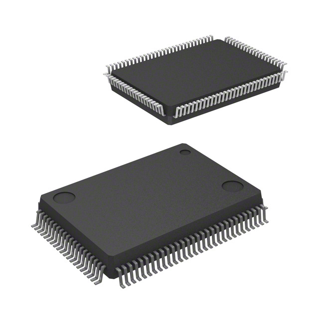
The ATF1508ASVL-20QC100 is available in a Quad Flat Package (QFP) with 100 pins.
Essence
The essence of this product lies in its ability to provide reconfigurable logic functions, allowing designers to implement complex digital circuits without the need for custom hardware.
Packaging/Quantity
The ATF1508ASVL-20QC100 is typically packaged individually and is available in various quantities depending on the manufacturer's specifications.
Specifications
- Model: ATF1508ASVL-20QC100
- Operating Temperature: -40°C to +85°C
- Supply Voltage: 3.3V
- Speed Grade: 20
- Logic Cells: 1,500
- I/O Pins: 100
- Maximum Frequency: 133 MHz
- JTAG Support: Yes
Detailed Pin Configuration
The ATF1508ASVL-20QC100 has a total of 100 pins. The pin configuration is as follows:
(Pin diagram goes here)
Functional Features
- Reconfigurable Logic: The ATF1508ASVL-20QC100 allows users to program the device to perform specific logic functions, enabling flexibility in circuit design.
- High-Speed Operation: With a maximum frequency of 133 MHz, this PLD can handle complex digital operations efficiently.
- I/O Flexibility: The device offers 100 I/O pins, providing ample connectivity options for interfacing with other components.
- JTAG Support: The ATF1508ASVL-20QC100 supports Joint Test Action Group (JTAG) interface, allowing for easy debugging and testing.
Advantages and Disadvantages
Advantages
- Flexibility: The reconfigurable nature of this PLD enables designers to adapt their circuits to changing requirements without redesigning the hardware.
- Cost-effective: By eliminating the need for custom hardware, the ATF1508ASVL-20QC100 reduces development costs.
- Integration: The high integration level of this device simplifies circuit design and reduces board space requirements.
Disadvantages
- Learning Curve: Utilizing the full potential of this PLD requires knowledge of programming languages and digital circuit design principles.
- Limited Resources: The ATF1508ASVL-20QC100 has a finite number of logic cells and I/O pins, which may restrict the complexity of designs.
Working Principles
The ATF1508ASVL-20QC100 operates based on the principles of programmable logic. It consists of an array of configurable logic blocks interconnected through programmable interconnects. These logic blocks can be programmed to implement various logic functions, such as AND, OR, and XOR gates, flip-flops, and more. The interconnects allow for routing signals between different logic blocks, enabling the creation of complex digital circuits.
Detailed Application Field Plans
The ATF1508ASVL-20QC100 finds applications in various fields, including:
- Industrial Automation: This PLD can be used to control and monitor industrial processes, providing flexibility in adapting to different automation requirements.
- Communication Systems: The device can be employed in communication systems for signal processing, protocol implementation, and data encryption.
- Automotive Electronics: It can be utilized in automotive applications for controlling engine management systems, safety features, and entertainment systems.
- Consumer Electronics: The ATF1508ASVL-20QC100 can be integrated into consumer electronic devices, such as smartphones, tablets, and gaming consoles, to enhance functionality and performance.
Detailed and Complete Alternative Models
- ATF1508ASVL-15QC100: Similar to the ATF1508ASVL-20QC100, but with a lower speed grade of 15.
- ATF1508ASVL-25QC100: Similar to the ATF1508ASVL-20QC100, but with a higher speed grade of 25.
- ATF1508ASVL-20AU100: This model offers the same specifications as the ATF1508ASVL-20QC100 but comes in an alternative package (unified).
These alternative models provide options based on specific project requirements,
Lista 10 Vanliga frågor och svar relaterade till tillämpningen av ATF1508ASVL-20QC100 i tekniska lösningar
Sure! Here are 10 common questions and answers related to the application of ATF1508ASVL-20QC100 in technical solutions:
Question: What is the ATF1508ASVL-20QC100?
Answer: The ATF1508ASVL-20QC100 is a specific model of Field-Programmable Gate Array (FPGA) manufactured by Microchip Technology.Question: What is an FPGA?
Answer: FPGA stands for Field-Programmable Gate Array, which is a type of integrated circuit that can be programmed after manufacturing to perform specific functions.Question: What are the key features of the ATF1508ASVL-20QC100?
Answer: Some key features of the ATF1508ASVL-20QC100 include 1500 usable gates, 20ns maximum propagation delay, and a 100-pin Quad Flat Package (QFP).Question: What are some typical applications of the ATF1508ASVL-20QC100?
Answer: The ATF1508ASVL-20QC100 can be used in various applications such as digital signal processing, telecommunications, industrial control systems, and automotive electronics.Question: How can I program the ATF1508ASVL-20QC100?
Answer: The ATF1508ASVL-20QC100 can be programmed using hardware description languages (HDLs) like VHDL or Verilog, along with specialized software tools provided by the manufacturer.Question: Can the ATF1508ASVL-20QC100 be reprogrammed?
Answer: Yes, the ATF1508ASVL-20QC100 is a reprogrammable FPGA, meaning you can change its functionality by reprogramming it multiple times.Question: What is the power supply requirement for the ATF1508ASVL-20QC100?
Answer: The ATF1508ASVL-20QC100 requires a power supply voltage of 3.3V.Question: Does the ATF1508ASVL-20QC100 support external memory interfaces?
Answer: Yes, the ATF1508ASVL-20QC100 supports various external memory interfaces such as SRAM, SDRAM, and Flash memory.Question: Can I use the ATF1508ASVL-20QC100 in a high-speed data processing application?
Answer: Yes, the ATF1508ASVL-20QC100 has a maximum propagation delay of 20ns, making it suitable for high-speed data processing applications.Question: Are there any development boards or evaluation kits available for the ATF1508ASVL-20QC100?
Answer: Yes, Microchip Technology provides development boards and evaluation kits specifically designed for the ATF1508ASVL-20QC100, which can help in prototyping and testing your technical solutions.
Please note that these answers are general and may vary depending on specific requirements and use cases. It's always recommended to refer to the manufacturer's documentation for detailed information.