

ATF1508ASV-15QC100
Product Overview
Category
ATF1508ASV-15QC100 belongs to the category of programmable logic devices (PLDs).
Use
This product is commonly used in digital circuit design and implementation. It provides a flexible and customizable solution for various applications.
Characteristics
- Programmable: The ATF1508ASV-15QC100 can be programmed to perform specific functions according to the user's requirements.
- High Integration: It integrates multiple logic gates, flip-flops, and other components into a single device, reducing the need for external components.
- Versatile: This PLD can be used in a wide range of applications due to its programmability.
- Low Power Consumption: The ATF1508ASV-15QC100 is designed to operate efficiently with low power consumption.
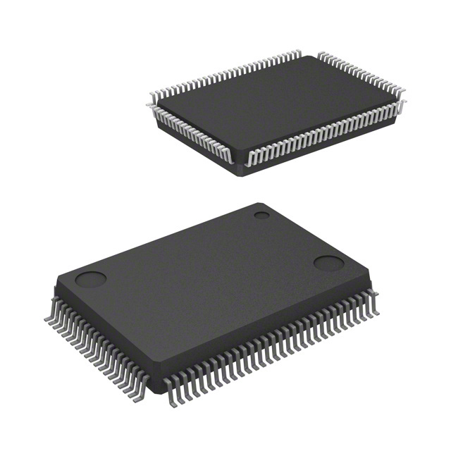
- Compact Package: It comes in a QC100 package, which is a small form factor suitable for space-constrained designs.
Packaging/Quantity
The ATF1508ASV-15QC100 is typically packaged in reels or tubes, containing a specified quantity of devices per package.
Specifications
- Device Type: ATF1508ASV-15QC100
- Logic Cells: 1508
- Speed Grade: -15
- Package Type: QC100
- Operating Voltage: 3.3V
- I/O Pins: 100
- Maximum Frequency: 125 MHz
- Programmable Logic Blocks: 84
- Macrocells: 64
- JTAG Support: Yes
Detailed Pin Configuration
The ATF1508ASV-15QC100 has a total of 100 pins. The pin configuration is as follows:
(Pin Number) (Pin Name) 1. VCCIO 2. GND 3. IO0 4. IO1 5. IO2 6. IO3 7. IO4 8. IO5 9. IO6 10. IO7 ... 100. IO99
Functional Features
- High-Speed Operation: The ATF1508ASV-15QC100 can operate at a maximum frequency of 125 MHz, enabling fast and efficient data processing.
- Flexible I/O Configuration: It offers a wide range of I/O pins, allowing for versatile connectivity options with external devices.
- JTAG Support: The device supports Joint Test Action Group (JTAG) interface, facilitating programming and debugging processes.
- In-System Programmability: The ATF1508ASV-15QC100 can be programmed while in operation, eliminating the need for physical reconfiguration.
Advantages and Disadvantages
Advantages
- Customizability: The ATF1508ASV-15QC100 allows users to create tailored logic designs to meet specific application requirements.
- Integration: It integrates multiple components into a single device, reducing the need for additional external components.
- Compact Size: The QC100 package ensures a small form factor, making it suitable for space-constrained designs.
- Low Power Consumption: The device operates efficiently with low power consumption, contributing to energy-saving applications.
Disadvantages
- Complexity: Programming and configuring the ATF1508ASV-15QC100 may require specialized knowledge and expertise.
- Limited Resources: The device has a finite number of logic cells and I/O pins, which may restrict the complexity and scale of designs.
Working Principles
The ATF1508ASV-15QC100 is based on programmable logic technology. It consists of configurable logic blocks, flip-flops, interconnects, and input/output circuitry. These components can be interconnected and programmed to implement various digital functions. The device's working principle involves configuring the internal connections and logic operations through programming tools, enabling the desired functionality.
Detailed Application Field Plans
The ATF1508ASV-15QC100 finds applications in various fields, including:
- Communications: It can be used in networking equipment, routers, and switches for data processing and control functions.
- Industrial Automation: The device is suitable for implementing control systems, motor drives, and sensor interfaces in industrial automation applications.
- Consumer Electronics: It can be utilized in consumer electronic devices such as gaming consoles, set-top boxes, and multimedia players for logic and interface functions.
- Automotive: The ATF1508ASV-15QC100 can be employed in automotive electronics for controlling engine management systems, dashboard displays, and safety features.
- Medical Devices: It finds application in medical equipment for signal processing, control, and data acquisition purposes.
Detailed and Complete Alternative Models
- ATF1508ASV-10QC100
- ATF1508ASV-20QC100
- ATF1508ASV-15JC84
- ATF1508ASV-15AU100
- ATF1508ASV-15AI100
These alternative models offer similar functionality
Lista 10 Vanliga frågor och svar relaterade till tillämpningen av ATF1508ASV-15QC100 i tekniska lösningar
Question: What is ATF1508ASV-15QC100?
Answer: ATF1508ASV-15QC100 is a specific model of Field Programmable Gate Array (FPGA) manufactured by Microchip Technology. It is commonly used in various technical solutions.Question: What are the key features of ATF1508ASV-15QC100?
Answer: Some key features of ATF1508ASV-15QC100 include 1500 usable gates, 8 macrocells, 64 input/output pins, and a maximum operating frequency of 15 MHz.Question: In what applications can ATF1508ASV-15QC100 be used?
Answer: ATF1508ASV-15QC100 can be used in a wide range of applications such as industrial control systems, automotive electronics, telecommunications, medical devices, and consumer electronics.Question: How can I program ATF1508ASV-15QC100?
Answer: ATF1508ASV-15QC100 can be programmed using industry-standard hardware description languages (HDL) such as VHDL or Verilog. Programming tools provided by Microchip Technology can be used to generate the programming file for the FPGA.Question: Can ATF1508ASV-15QC100 be reprogrammed after it has been programmed once?
Answer: Yes, ATF1508ASV-15QC100 is a field-programmable device, which means it can be reprogrammed multiple times to implement different designs or make modifications to the existing design.Question: What is the power supply requirement for ATF1508ASV-15QC100?
Answer: ATF1508ASV-15QC100 requires a single power supply voltage of 5 volts (Vcc).Question: Does ATF1508ASV-15QC100 support external memory interfaces?
Answer: Yes, ATF1508ASV-15QC100 supports external memory interfaces such as SRAM, SDRAM, and Flash memory. It can be used to interface with external memory devices for data storage or retrieval.Question: Can ATF1508ASV-15QC100 communicate with other devices or microcontrollers?
Answer: Yes, ATF1508ASV-15QC100 has multiple input/output pins that can be used for communication with other devices or microcontrollers using various protocols such as UART, SPI, I2C, or custom protocols.Question: What is the maximum operating temperature range for ATF1508ASV-15QC100?
Answer: The maximum operating temperature range for ATF1508ASV-15QC100 is typically -40°C to +85°C.Question: Are there any application notes or reference designs available for ATF1508ASV-15QC100?
Answer: Yes, Microchip Technology provides application notes, reference designs, and technical documentation on their website that can help in understanding and implementing ATF1508ASV-15QC100 in various technical solutions.