

MAX197BENI+ - English Editing Encyclopedia Entry
Product Overview
Category
MAX197BENI+ belongs to the category of integrated circuits (ICs).
Use
It is primarily used for analog-to-digital conversion in various electronic devices.
Characteristics
- High precision and accuracy
- Low power consumption
- Wide operating voltage range
- Small form factor
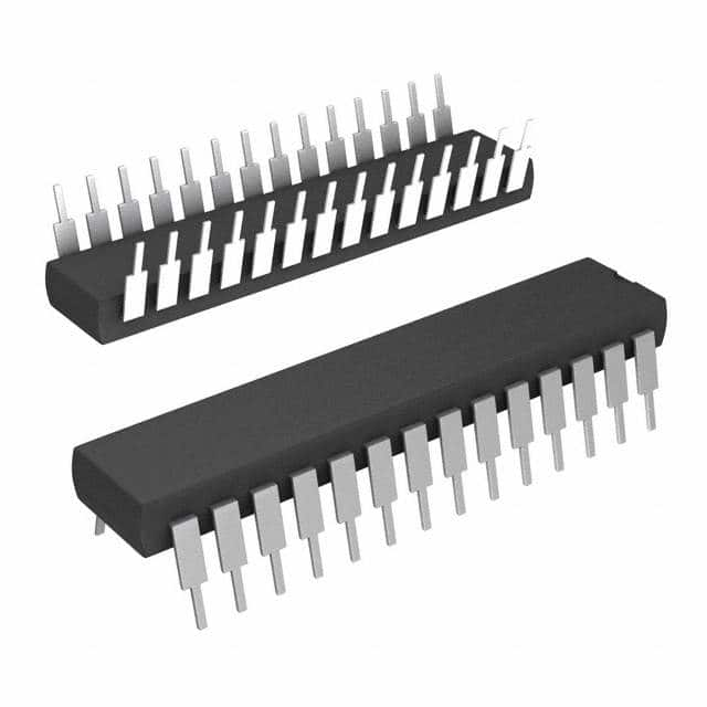
Package
The MAX197BENI+ comes in a compact package, making it suitable for space-constrained applications.
Essence
The essence of MAX197BENI+ lies in its ability to convert analog signals into digital data with high fidelity.
Packaging/Quantity
This product is typically packaged in reels or tubes, with a quantity of 250 units per reel/tube.
Specifications
- Resolution: 12 bits
- Input Voltage Range: 0V to Vref
- Conversion Time: 1.6µs (typical)
- Operating Temperature Range: -40°C to +85°C
- Supply Voltage Range: 2.7V to 5.25V
Detailed Pin Configuration
The MAX197BENI+ has a total of 16 pins, each serving a specific function. The pin configuration is as follows:
- VDD - Positive supply voltage
- VREF - Reference voltage input
- AGND - Analog ground
- REFOUT - Reference voltage output
- IN+ - Positive analog input
- IN- - Negative analog input
- DGND - Digital ground
- CS - Chip select input
- SCLK - Serial clock input
- SDATA - Serial data input/output
- EOC - End of conversion output
- SHDN - Shutdown control input
- NC - No connection
- NC - No connection
- NC - No connection
- VSS - Negative supply voltage
Functional Features
- High-resolution analog-to-digital conversion
- Serial interface for easy integration with microcontrollers
- Low power consumption for energy-efficient designs
- Shutdown mode for power-saving when not in use
- End of conversion signal for synchronization with external devices
Advantages and Disadvantages
Advantages
- High precision and accuracy in analog-to-digital conversion
- Wide operating voltage range allows for versatile applications
- Small form factor enables integration into compact electronic devices
- Low power consumption for energy-efficient operation
Disadvantages
- Limited resolution compared to higher-end ADCs
- May require additional external components for specific applications
Working Principles
The MAX197BENI+ utilizes a successive approximation register (SAR) architecture to convert analog signals into digital data. It employs an internal reference voltage and compares the input voltage to this reference using a series of binary comparisons. The result is a digital representation of the analog input.
Detailed Application Field Plans
The MAX197BENI+ finds applications in various fields, including but not limited to: - Industrial automation - Medical devices - Test and measurement equipment - Consumer electronics - Automotive systems
Detailed and Complete Alternative Models
- MAX11100 - 12-bit SAR ADC with integrated reference and temperature sensor
- ADS1115 - 16-bit I2C-compatible ADC with programmable gain amplifier
- LTC1867 - 16-bit SAR ADC with differential inputs and high-speed sampling rate
- MCP3208 - 12-bit SPI ADC with 8 channels and low power consumption
- AD7091R - 12-bit SAR ADC with on-chip reference and temperature sensor
These alternative models offer similar functionality and can be considered as alternatives to the MAX197BENI+ based on specific requirements and design constraints.
In conclusion, the MAX197BENI+ is a high-precision analog-to-digital converter with various features and advantages. Its compact size and low power consumption make it suitable for a wide range of applications in different industries.
Lista 10 Vanliga frågor och svar relaterade till tillämpningen av MAX197BENI+ i tekniska lösningar
Sure! Here are 10 common questions and answers related to the application of MAX197BENI+ in technical solutions:
Q: What is the MAX197BENI+? A: The MAX197BENI+ is a 12-bit, low-power, serial-output analog-to-digital converter (ADC) that can be used in various technical applications.
Q: What is the supply voltage range for the MAX197BENI+? A: The supply voltage range for the MAX197BENI+ is typically between 2.7V and 5.25V.
Q: How many analog input channels does the MAX197BENI+ have? A: The MAX197BENI+ has 8 single-ended analog input channels.
Q: What is the maximum sampling rate of the MAX197BENI+? A: The maximum sampling rate of the MAX197BENI+ is 200 kilosamples per second (ksps).
Q: Can the MAX197BENI+ operate in both single-ended and differential modes? A: Yes, the MAX197BENI+ can operate in both single-ended and differential modes, providing flexibility in different applications.
Q: What is the resolution of the MAX197BENI+? A: The MAX197BENI+ has a resolution of 12 bits, allowing for precise analog-to-digital conversion.
Q: Does the MAX197BENI+ have an internal reference voltage? A: No, the MAX197BENI+ does not have an internal reference voltage. An external reference voltage must be provided.
Q: Is the MAX197BENI+ compatible with microcontrollers and other digital devices? A: Yes, the MAX197BENI+ is compatible with microcontrollers and other digital devices through its serial interface.
Q: Can the MAX197BENI+ be used in battery-powered applications? A: Yes, the MAX197BENI+ is designed for low-power operation, making it suitable for battery-powered applications.
Q: Are there any evaluation kits or development tools available for the MAX197BENI+? A: Yes, Maxim Integrated provides evaluation kits and development tools to help users easily integrate the MAX197BENI+ into their designs.
Please note that these answers are general and may vary depending on specific application requirements and datasheet specifications.