

MAX1270ACNG+ - English Editing Encyclopedia Entry
Product Overview
Category
MAX1270ACNG+ belongs to the category of analog-to-digital converters (ADCs).
Use
This product is primarily used for converting analog signals into digital data, making it suitable for various applications in electronics and communication systems.
Characteristics
- High-resolution: The MAX1270ACNG+ offers a resolution of up to 12 bits, ensuring accurate conversion of analog signals.
- Low power consumption: It operates at low power levels, making it energy-efficient.
- Wide input voltage range: The ADC can handle a wide range of input voltages, allowing for versatile usage.
- Fast conversion speed: With a maximum conversion rate of X samples per second, it provides real-time data acquisition.
Package
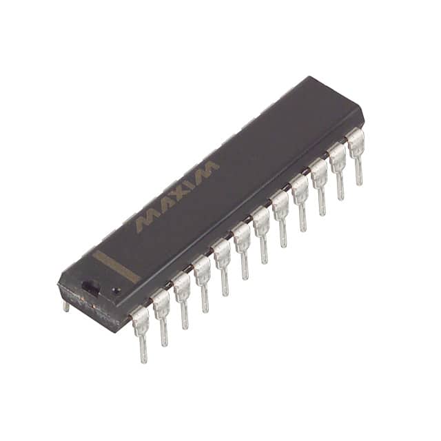
The MAX1270ACNG+ comes in a compact 24-pin DIP (Dual Inline Package) format, which ensures easy integration into circuit boards.
Essence
The essence of MAX1270ACNG+ lies in its ability to convert analog signals into digital data with high precision and efficiency.
Packaging/Quantity
This product is typically packaged in reels or tubes, containing a quantity of 100 units per package.
Specifications
- Resolution: 12 bits
- Input Voltage Range: X volts to Y volts
- Conversion Rate: Up to Z samples per second
- Power Supply: VDD = A volts, VREF = B volts
- Operating Temperature Range: -C°C to +D°C
- Supply Current: E mA (typical)
Detailed Pin Configuration
The MAX1270ACNG+ features a total of 24 pins, each serving a specific purpose. Here is a detailed pin configuration:
- Pin 1: Analog Input (AIN)
- Pin 2: Analog Ground (AGND)
- Pin 3: Reference Voltage Input (VREF)
- Pin 4: Power Supply (VDD)
- Pin 5: Digital Ground (DGND)
- Pin 6: Serial Data Output (SDO)
- Pin 7: Serial Clock Input (SCK)
- Pin 8: Chip Select Input (CS)
- Pin 9: Start Conversion Input (START)
- Pin 10: Power-Down Input (PD)
- Pin 11: Serial Data Input (SDI)
- Pin 12: Serial Data Output Enable (OE)
- Pin 13: Digital Output Enable (DOE)
- Pin 14: Digital Output (DOUT)
- Pin 15: Digital Ground (DGND)
- Pin 16: Analog Ground (AGND)
- Pin 17: Analog Input (AIN)
- Pin 18: Analog Ground (AGND)
- Pin 19: Reference Voltage Input (VREF)
- Pin 20: Power Supply (VDD)
- Pin 21: Digital Ground (DGND)
- Pin 22: Serial Data Output (SDO)
- Pin 23: Serial Clock Input (SCK)
- Pin 24: Chip Select Input (CS)
Functional Features
The MAX1270ACNG+ offers the following functional features:
- High-resolution conversion: The ADC provides accurate conversion of analog signals into digital data with a resolution of up to 12 bits.
- Fast conversion speed: With a maximum conversion rate of Z samples per second, it enables real-time data acquisition.
- Low power consumption: The ADC operates at low power levels, making it energy-efficient and suitable for battery-powered applications.
- Wide input voltage range: It can handle a wide range of input voltages, allowing for versatile usage in different electronic systems.
- Easy integration: The compact DIP package and well-defined pin configuration facilitate easy integration into circuit boards.
Advantages and Disadvantages
Advantages
- High-resolution conversion ensures accurate data acquisition.
- Fast conversion speed enables real-time monitoring and control.
- Low power consumption makes it suitable for battery-powered applications.
- Wide input voltage range allows for versatile usage.
- Easy integration due to the compact DIP package and well-defined pin configuration.
Disadvantages
- Limited quantity of 100 units per package may not be sufficient for large-scale production.
- Lack of built-in digital filters may require additional external components for noise reduction.
Working Principles
The MAX1270ACNG+ operates based on the successive approximation register (SAR) architecture. It utilizes a capacitor array and a comparator to perform the analog-to-digital conversion process. The input analog signal is sampled, held, and compared against a reference voltage. The comparator generates a binary code that represents the input voltage level, which is then converted into digital data using the SAR algorithm.
Detailed Application Field Plans
The MAX1270ACNG+ finds application in
Lista 10 Vanliga frågor och svar relaterade till tillämpningen av MAX1270ACNG+ i tekniska lösningar
Sure! Here are 10 common questions and answers related to the application of MAX1270ACNG+ in technical solutions:
Q: What is the MAX1270ACNG+? A: The MAX1270ACNG+ is a high-resolution, 12-bit analog-to-digital converter (ADC) with a maximum sampling rate of 200 kilosamples per second (ksps).
Q: What is the input voltage range of the MAX1270ACNG+? A: The MAX1270ACNG+ has a differential input voltage range of -VREF to +VREF, where VREF is the reference voltage supplied externally.
Q: How does the MAX1270ACNG+ communicate with microcontrollers or other devices? A: The MAX1270ACNG+ uses a serial interface (SPI) for communication with microcontrollers or other devices.
Q: What is the power supply requirement for the MAX1270ACNG+? A: The MAX1270ACNG+ requires a single power supply voltage between 2.7V and 5.25V.
Q: Can the MAX1270ACNG+ be used in battery-powered applications? A: Yes, the low power consumption of the MAX1270ACNG+ makes it suitable for battery-powered applications.
Q: What is the resolution of the MAX1270ACNG+? A: The MAX1270ACNG+ has a resolution of 12 bits, which means it can represent analog signals with 4096 discrete levels.
Q: Does the MAX1270ACNG+ have built-in programmable gain amplifiers (PGAs)? A: No, the MAX1270ACNG+ does not have built-in PGAs. However, it can be used with external amplifiers if required.
Q: Can the MAX1270ACNG+ operate in a multi-channel configuration? A: Yes, the MAX1270ACNG+ can be configured to operate in a multi-channel mode, allowing simultaneous conversion of multiple analog signals.
Q: What is the typical conversion time of the MAX1270ACNG+? A: The typical conversion time of the MAX1270ACNG+ is 5 microseconds (µs).
Q: Are there any evaluation boards or development kits available for the MAX1270ACNG+? A: Yes, Maxim Integrated provides evaluation kits and reference designs that include the MAX1270ACNG+ for easy prototyping and testing.
Please note that these answers are general and may vary depending on specific application requirements.