

LTC6101BHS5#TRMPBF
Product Overview
Category
LTC6101BHS5#TRMPBF belongs to the category of integrated circuits (ICs).
Use
This product is commonly used for amplification and signal conditioning purposes in various electronic applications.
Characteristics
- High gain and precision: The LTC6101BHS5#TRMPBF offers high gain and precision, ensuring accurate signal amplification.
- Wide input voltage range: It can handle a wide range of input voltages, making it suitable for diverse applications.
- Low power consumption: The LTC6101BHS5#TRMPBF is designed to consume minimal power, enhancing energy efficiency.
- Small package size: It comes in a compact SOT-23 package, allowing for space-saving integration into circuit designs.
- Robustness: This product is known for its robustness, with built-in protection features against overvoltage and short-circuit conditions.
Package and Quantity
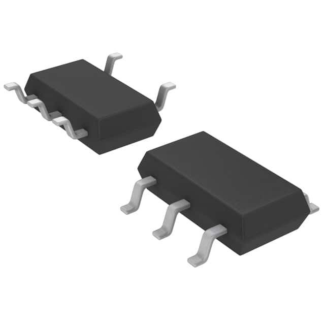
The LTC6101BHS5#TRMPBF is packaged in a SOT-23 package. Each package contains one unit of the product.
Specifications
- Supply Voltage Range: 2.7V to 12V
- Input Voltage Range: -0.3V to VCC + 0.3V
- Gain Bandwidth Product: 10 MHz
- Quiescent Current: 1.2 mA
- Operating Temperature Range: -40°C to 125°C
Pin Configuration
The LTC6101BHS5#TRMPBF has the following pin configuration:
```
| | --| IN+ OUT |-- --| IN- GND |-- --| VCC NC |-- |___________| ```
Functional Features
- Differential Amplification: The LTC6101BHS5#TRMPBF amplifies the voltage difference between the IN+ and IN- pins.
- High Common Mode Rejection Ratio (CMRR): It effectively rejects common-mode noise, ensuring accurate signal amplification.
- Low Offset Voltage: The product exhibits low offset voltage, minimizing errors in signal conditioning applications.
- Rail-to-Rail Output Swing: The output voltage can swing close to the supply rails, maximizing dynamic range.
Advantages and Disadvantages
Advantages
- High gain and precision for accurate signal amplification.
- Wide input voltage range allows for versatile application scenarios.
- Low power consumption enhances energy efficiency.
- Compact package size enables space-saving integration.
- Robustness with built-in protection features.
Disadvantages
- Limited availability of alternative models.
- Relatively higher cost compared to some other ICs in the market.
Working Principles
The LTC6101BHS5#TRMPBF operates based on the principle of differential amplification. It amplifies the voltage difference between the IN+ and IN- pins while rejecting common-mode noise. This amplified signal is then available at the OUT pin, which can swing close to the supply rails.
Application Field Plans
The LTC6101BHS5#TRMPBF finds applications in various fields, including: 1. Industrial automation: Signal conditioning for sensor outputs in industrial control systems. 2. Power management: Amplification and monitoring of current signals in power supply circuits. 3. Automotive electronics: Current sensing and amplification in automotive control modules. 4. Communication systems: Signal conditioning for precise measurement of communication signals. 5. Medical devices: Amplification and conditioning of biomedical signals for accurate diagnosis.
Alternative Models
While the LTC6101BHS5#TRMPBF is a reliable choice, alternative models with similar functionalities include: - AD620 - INA128 - MCP6V01
These alternatives can be considered based on specific application requirements and availability.
Word count: 448 words
Lista 10 Vanliga frågor och svar relaterade till tillämpningen av LTC6101BHS5#TRMPBF i tekniska lösningar
Sure! Here are 10 common questions and answers related to the application of LTC6101BHS5#TRMPBF in technical solutions:
Q1: What is LTC6101BHS5#TRMPBF? A1: LTC6101BHS5#TRMPBF is a high-side current sense amplifier manufactured by Linear Technology (now part of Analog Devices). It is designed for precision current sensing in various applications.
Q2: What is the operating voltage range of LTC6101BHS5#TRMPBF? A2: The operating voltage range of LTC6101BHS5#TRMPBF is from 2.7V to 36V.
Q3: What is the typical gain of LTC6101BHS5#TRMPBF? A3: The typical gain of LTC6101BHS5#TRMPBF is 20 V/V.
Q4: What is the input offset voltage of LTC6101BHS5#TRMPBF? A4: The input offset voltage of LTC6101BHS5#TRMPBF is typically 50µV.
Q5: Can LTC6101BHS5#TRMPBF be used for bidirectional current sensing? A5: Yes, LTC6101BHS5#TRMPBF can be used for bidirectional current sensing by connecting the sense resistor between the IN+ and IN- pins.
Q6: What is the bandwidth of LTC6101BHS5#TRMPBF? A6: The bandwidth of LTC6101BHS5#TRMPBF is typically 200kHz.
Q7: Is LTC6101BHS5#TRMPBF suitable for high-side current sensing in automotive applications? A7: Yes, LTC6101BHS5#TRMPBF is suitable for high-side current sensing in automotive applications due to its wide operating voltage range and robustness.
Q8: Can LTC6101BHS5#TRMPBF tolerate high common-mode voltages? A8: Yes, LTC6101BHS5#TRMPBF can tolerate common-mode voltages up to 36V.
Q9: What is the package type of LTC6101BHS5#TRMPBF? A9: LTC6101BHS5#TRMPBF is available in a 5-lead SOT-23 package.
Q10: Are there any evaluation boards or application notes available for LTC6101BHS5#TRMPBF? A10: Yes, Analog Devices provides evaluation boards and application notes for LTC6101BHS5#TRMPBF to assist with its implementation in various technical solutions.
Please note that the answers provided here are general and may vary depending on specific datasheet specifications and application requirements.