

LT6108IDCB-2#TRMPBF
Product Overview
Category
The LT6108IDCB-2#TRMPBF belongs to the category of integrated circuits (ICs).
Use
This product is commonly used in electronic devices for signal conditioning and amplification purposes.
Characteristics
- The LT6108IDCB-2#TRMPBF is a high precision, low power, dual operational amplifier.
- It operates over a wide temperature range and has excellent DC performance.
- This IC offers low input offset voltage, low input bias current, and low noise characteristics.
- It is designed to provide accurate amplification and filtering of signals in various applications.
Package
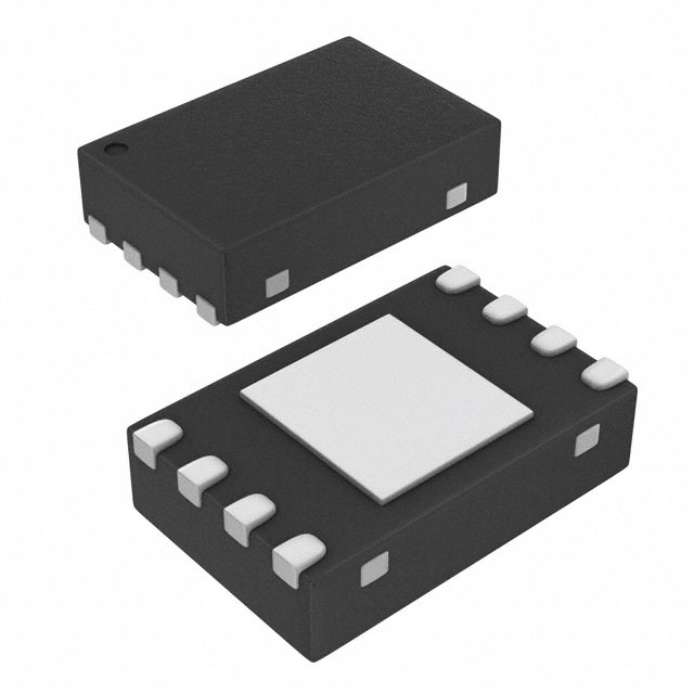
The LT6108IDCB-2#TRMPBF is available in a small form factor package, specifically the DFN-10 (3mm x 3mm) package.
Essence
The essence of this product lies in its ability to accurately amplify and condition signals while consuming minimal power.
Packaging/Quantity
The LT6108IDCB-2#TRMPBF is typically packaged in reels or tubes, with each reel or tube containing a specific quantity of ICs. The exact quantity may vary depending on the manufacturer's specifications.
Specifications
- Supply Voltage: 2.7V to 36V
- Input Offset Voltage: ±150µV (maximum)
- Input Bias Current: ±20nA (maximum)
- Gain Bandwidth Product: 1MHz (typical)
- Operating Temperature Range: -40°C to 125°C
Detailed Pin Configuration
The LT6108IDCB-2#TRMPBF has a total of 10 pins, which are assigned specific functions as follows:
- OUT1: Output 1
- IN1-: Inverting Input 1
- IN1+: Non-Inverting Input 1
- V-: Negative Power Supply
- V+: Positive Power Supply
- IN2+: Non-Inverting Input 2
- IN2-: Inverting Input 2
- OUT2: Output 2
- NC: No Connection
- GND: Ground
Functional Features
- High precision amplification of signals with low offset voltage and bias current.
- Wide operating voltage range allows for flexibility in various applications.
- Low power consumption makes it suitable for battery-powered devices.
- Excellent DC performance ensures accurate signal conditioning.
Advantages and Disadvantages
Advantages
- High precision amplification
- Low power consumption
- Wide operating voltage range
- Excellent DC performance
Disadvantages
- Limited gain bandwidth product compared to some other ICs in the same category
- May require additional external components for specific applications
Working Principles
The LT6108IDCB-2#TRMPBF operates based on the principles of operational amplifiers. It amplifies the difference between the voltages at its non-inverting and inverting inputs, providing a high gain output signal. The IC is designed to minimize input offset voltage and bias current, ensuring accurate amplification of signals.
Detailed Application Field Plans
The LT6108IDCB-2#TRMPBF finds applications in various fields, including but not limited to: - Industrial automation - Medical equipment - Test and measurement instruments - Audio amplification systems - Sensor signal conditioning
Detailed and Complete Alternative Models
Some alternative models that offer similar functionality to the LT6108IDCB-2#TRMPBF include: - AD8628 - MCP6022 - MAX44246
These alternative models can be considered based on specific application requirements and desired specifications.
Word count: 445 words
Lista 10 Vanliga frågor och svar relaterade till tillämpningen av LT6108IDCB-2#TRMPBF i tekniska lösningar
Sure! Here are 10 common questions and answers related to the application of LT6108IDCB-2#TRMPBF in technical solutions:
Question: What is the LT6108IDCB-2#TRMPBF?
Answer: The LT6108IDCB-2#TRMPBF is a high voltage, precision current sense amplifier designed for use in various technical applications.Question: What is the input voltage range of the LT6108IDCB-2#TRMPBF?
Answer: The LT6108IDCB-2#TRMPBF has an input voltage range of -0.3V to 44V.Question: What is the output voltage range of the LT6108IDCB-2#TRMPBF?
Answer: The LT6108IDCB-2#TRMPBF has an output voltage range of 0V to 5V.Question: What is the typical gain of the LT6108IDCB-2#TRMPBF?
Answer: The typical gain of the LT6108IDCB-2#TRMPBF is 20V/V.Question: Can the LT6108IDCB-2#TRMPBF be used in high voltage applications?
Answer: Yes, the LT6108IDCB-2#TRMPBF is specifically designed for high voltage applications.Question: What is the supply voltage range of the LT6108IDCB-2#TRMPBF?
Answer: The supply voltage range of the LT6108IDCB-2#TRMPBF is 2.85V to 36V.Question: Is the LT6108IDCB-2#TRMPBF suitable for current sensing in power management systems?
Answer: Yes, the LT6108IDCB-2#TRMPBF is commonly used for current sensing in power management systems.Question: Does the LT6108IDCB-2#TRMPBF have built-in protection features?
Answer: Yes, the LT6108IDCB-2#TRMPBF has built-in fault detection and protection features to ensure safe operation.Question: Can the LT6108IDCB-2#TRMPBF be used in automotive applications?
Answer: Yes, the LT6108IDCB-2#TRMPBF is suitable for automotive applications due to its high voltage capability and robust design.Question: What is the package type of the LT6108IDCB-2#TRMPBF?
Answer: The LT6108IDCB-2#TRMPBF is available in a 6-pin DFN package.
Please note that these answers are general and may vary depending on specific application requirements. It is always recommended to refer to the datasheet and consult with technical experts for accurate information.