

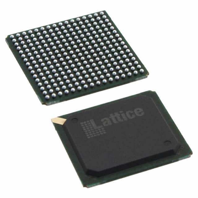
LFXP6E-3F256I
Product Overview
Category
The LFXP6E-3F256I belongs to the category of Field-Programmable Gate Arrays (FPGAs).
Use
FPGAs are integrated circuits that can be programmed and reprogrammed to perform various digital functions. The LFXP6E-3F256I is specifically designed for applications requiring high-performance and low-power consumption.
Characteristics
- High-performance FPGA with low power consumption
- Programmable and reprogrammable functionality
- Suitable for a wide range of applications
- Compact package size
Package
The LFXP6E-3F256I comes in a small form factor package, making it suitable for space-constrained designs.
Essence
The essence of the LFXP6E-3F256I lies in its ability to provide flexible and customizable digital logic functions, enabling designers to implement complex systems on a single chip.
Packaging/Quantity
The LFXP6E-3F256I is typically packaged in trays or reels, with a quantity of 250 units per package.
Specifications
- Logic Cells: 6,080
- Flip-Flops: 12,160
- Block RAM: 288 Kbits
- DSP Slices: 48
- Maximum Frequency: 400 MHz
- Operating Voltage: 1.2V
- I/O Pins: 256
- Configuration Memory: 256 Mbits
Detailed Pin Configuration
The LFXP6E-3F256I has a total of 256 I/O pins, which can be configured as inputs or outputs based on the application requirements. These pins are distributed across the device and can be accessed through the package's pinout.
For a detailed pin configuration diagram, please refer to the manufacturer's datasheet.
Functional Features
- High-performance FPGA architecture
- Low power consumption
- Flexible and customizable logic functions
- Support for various I/O standards
- On-chip memory resources for data storage
- Dedicated DSP slices for signal processing tasks
- Built-in configuration memory for easy reprogramming
Advantages and Disadvantages
Advantages
- Versatile and adaptable to different applications
- Allows for rapid prototyping and development
- Reduces time-to-market for complex digital systems
- Offers high performance with low power consumption
- Provides flexibility for future design iterations
Disadvantages
- Relatively higher cost compared to other programmable logic devices
- Steeper learning curve for beginners due to its complexity
- Limited availability of alternative models from other manufacturers
Working Principles
The LFXP6E-3F256I operates based on the principles of field-programmable gate arrays. It consists of a matrix of configurable logic blocks interconnected through programmable routing resources. The device can be programmed using hardware description languages (HDL) or graphical tools, allowing designers to define the desired functionality.
Once programmed, the LFXP6E-3F256I executes the specified logic functions, enabling the implementation of complex digital systems. The device can be reprogrammed as needed, providing flexibility for design changes or updates.
Detailed Application Field Plans
The LFXP6E-3F256I finds application in various fields, including:
- Communications: Used in wireless base stations, network routers, and optical communication systems.
- Industrial Automation: Employed in control systems, robotics, and factory automation.
- Automotive: Utilized in advanced driver-assistance systems (ADAS), infotainment systems, and engine control units (ECUs).
- Aerospace and Defense: Applied in radar systems, avionics, and secure communications.
- Medical Devices: Integrated into medical imaging equipment, patient monitoring systems, and laboratory instruments.
Detailed and Complete Alternative Models
While the LFXP6E-3F256I offers excellent performance and features, alternative models from other manufacturers can also be considered. Some notable alternatives include:
- Xilinx Artix-7 FPGA
- Intel Cyclone V FPGA
- Microchip PolarFire FPGA
- Lattice ECP5 FPGA
- Altera MAX 10 FPGA
These alternative models provide similar functionality and are widely used in various applications.
In conclusion, the LFXP6E-3F256I is a high-performance FPGA that offers flexibility, low power consumption, and a compact package size. It finds application in diverse fields and can be programmed to meet specific requirements. While it has advantages such as versatility and rapid prototyping, it also has disadvantages like higher cost and complexity. Designers can consider alternative models based on their specific needs.
Lista 10 Vanliga frågor och svar relaterade till tillämpningen av LFXP6E-3F256I i tekniska lösningar
Sure! Here are 10 common questions and answers related to the application of LFXP6E-3F256I in technical solutions:
Q: What is the LFXP6E-3F256I? A: The LFXP6E-3F256I is a field-programmable gate array (FPGA) manufactured by Lattice Semiconductor.
Q: What are the key features of the LFXP6E-3F256I? A: The LFXP6E-3F256I features 6,080 Look-Up Tables (LUTs), 128 Kbits of embedded block RAM, and 120 user I/O pins.
Q: What is the maximum operating frequency of the LFXP6E-3F256I? A: The LFXP6E-3F256I can operate at a maximum frequency of up to 300 MHz.
Q: What applications can the LFXP6E-3F256I be used for? A: The LFXP6E-3F256I can be used in various applications such as industrial automation, telecommunications, automotive, and consumer electronics.
Q: How can I program the LFXP6E-3F256I? A: The LFXP6E-3F256I can be programmed using Lattice Diamond or Lattice Radiant software tools.
Q: What voltage levels does the LFXP6E-3F256I support? A: The LFXP6E-3F256I supports both 3.3V and 1.2V voltage levels.
Q: Can the LFXP6E-3F256I interface with other devices? A: Yes, the LFXP6E-3F256I supports various interfaces such as SPI, I2C, UART, and GPIO.
Q: What is the power consumption of the LFXP6E-3F256I? A: The power consumption of the LFXP6E-3F256I depends on the design and configuration but typically ranges from 100mW to 1W.
Q: Can the LFXP6E-3F256I be used in high-reliability applications? A: Yes, the LFXP6E-3F256I is designed to meet the requirements of high-reliability applications and has built-in error detection and correction features.
Q: Where can I find more information about the LFXP6E-3F256I? A: You can find more detailed information about the LFXP6E-3F256I in the datasheet provided by Lattice Semiconductor or on their official website.
Please note that the answers provided here are general and may vary depending on specific use cases and requirements. It is always recommended to refer to the official documentation for accurate and up-to-date information.