

LFXP2-5E-6FT256I
Product Overview
Category
The LFXP2-5E-6FT256I belongs to the category of Field-Programmable Gate Arrays (FPGAs).
Use
FPGAs are integrated circuits that can be programmed and reprogrammed to perform various digital functions. The LFXP2-5E-6FT256I is specifically designed for applications requiring high-performance and low-power consumption.
Characteristics
- High performance: The LFXP2-5E-6FT256I offers a high logic density and fast processing capabilities, making it suitable for complex digital designs.
- Low power consumption: This FPGA is designed to minimize power usage, making it energy-efficient.
- Programmability: The LFXP2-5E-6FT256I can be easily programmed and reconfigured to adapt to different application requirements.
- Small form factor: It comes in a compact package, allowing for space-saving integration into electronic systems.
Package and Quantity
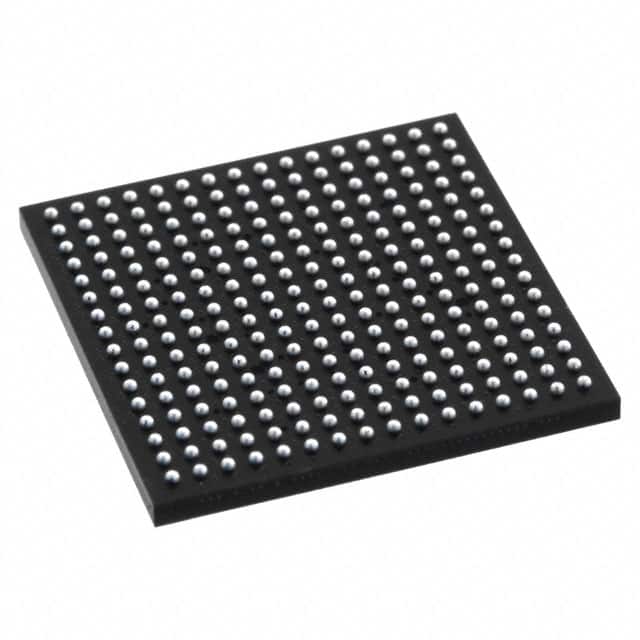
The LFXP2-5E-6FT256I is available in a 256-pin FineLine BGA (Ball Grid Array) package. It is typically sold individually or in small quantities.
Specifications
- Logic Cells: 5,120
- Flip-Flops: 10,240
- Block RAM: 288 Kbits
- Maximum Frequency: 400 MHz
- I/O Pins: 208
- Operating Voltage: 1.2V
- Configuration Memory: Flash-based
Detailed Pin Configuration
For a detailed pin configuration diagram of the LFXP2-5E-6FT256I, please refer to the manufacturer's datasheet.
Functional Features
- High-speed data processing: The LFXP2-5E-6FT256I can handle complex algorithms and data-intensive tasks efficiently.
- Flexible I/O capabilities: It offers a wide range of I/O options, allowing for seamless integration with other components and peripherals.
- On-chip memory: The built-in block RAM provides fast and reliable data storage for intermediate results and lookup tables.
- Clock management: The FPGA includes dedicated clocking resources to ensure precise timing control.
Advantages and Disadvantages
Advantages
- Versatility: The LFXP2-5E-6FT256I can be customized to meet specific application requirements, offering flexibility in design.
- High performance: It delivers fast processing speeds and high logic density, enabling the implementation of complex algorithms.
- Low power consumption: The FPGA's efficient power usage makes it suitable for battery-powered devices and energy-conscious applications.
Disadvantages
- Complexity: Programming and configuring FPGAs require specialized knowledge and expertise.
- Cost: FPGAs tend to be more expensive compared to other integrated circuits due to their programmability and versatility.
Working Principles
FPGAs consist of an array of configurable logic blocks interconnected by programmable routing channels. The LFXP2-5E-6FT256I utilizes a Flash-based configuration memory that stores the user-defined logic functions and interconnections. During operation, the FPGA executes the programmed instructions, performing the desired digital functions.
Detailed Application Field Plans
The LFXP2-5E-6FT256I finds applications in various fields, including:
- Communications: It can be used in networking equipment, routers, and switches to handle data processing and protocol conversion.
- Industrial Automation: The FPGA enables real-time control and monitoring in industrial automation systems, improving efficiency and reliability.
- Medical Devices: It can be employed in medical imaging, patient monitoring, and diagnostic equipment to process and analyze data.
- Aerospace and Defense: The FPGA's high-performance capabilities make it suitable for radar systems, avionics, and military applications.
- Automotive: It can be utilized in advanced driver-assistance systems (ADAS), infotainment systems, and engine control units (ECUs).
Detailed and Complete Alternative Models
- LFXP2-17E-6FT256I: A higher-density FPGA with 17,280 logic cells and 34,560 flip-flops.
- LFXP2-30E-6FT256I: An FPGA with increased logic capacity, offering 30,720 logic cells and 61,440 flip-flops.
- LFXP2-50E-6FT256I: A larger FPGA with 50,176 logic cells and 100,352 flip-flops, suitable for complex designs.
These alternative models provide a range of options with varying logic capacities to accommodate different project requirements.
In conclusion, the LFXP2-5E-6FT256I is a high-performance and low-power FPGA that offers versatility and flexibility in digital design. Its compact form factor and efficient power usage make it suitable for a wide range of applications across various industries
Lista 10 Vanliga frågor och svar relaterade till tillämpningen av LFXP2-5E-6FT256I i tekniska lösningar
Sure! Here are 10 common questions and answers related to the application of LFXP2-5E-6FT256I in technical solutions:
1. What is the LFXP2-5E-6FT256I? The LFXP2-5E-6FT256I is a field-programmable gate array (FPGA) manufactured by Lattice Semiconductor. It is designed for use in various technical solutions that require programmable logic.
2. What are the key features of the LFXP2-5E-6FT256I? Some key features of the LFXP2-5E-6FT256I include 5,120 Look-Up Tables (LUTs), 128 Kbits of embedded block RAM, 96 user I/O pins, and support for various I/O standards.
3. What applications can the LFXP2-5E-6FT256I be used for? The LFXP2-5E-6FT256I can be used in a wide range of applications such as industrial automation, communications, automotive electronics, medical devices, and more.
4. How can I program the LFXP2-5E-6FT256I? You can program the LFXP2-5E-6FT256I using Lattice Diamond or Lattice Radiant software tools provided by Lattice Semiconductor. These tools allow you to design and implement your desired logic functions.
5. What voltage levels does the LFXP2-5E-6FT256I support? The LFXP2-5E-6FT256I supports a wide range of voltage levels, including 1.2V, 1.5V, 1.8V, 2.5V, 3.3V, and 5V, making it compatible with various system requirements.
6. Can I use the LFXP2-5E-6FT256I in a high-reliability application? Yes, the LFXP2-5E-6FT256I is designed to meet the requirements of high-reliability applications. It has built-in features like error detection and correction, redundancy, and fault tolerance.
7. How can I interface the LFXP2-5E-6FT256I with other components or devices? The LFXP2-5E-6FT256I provides 96 user I/O pins that can be configured to support various communication protocols such as SPI, I2C, UART, and more. You can also use external interfaces like LVDS or differential signaling.
8. What is the power consumption of the LFXP2-5E-6FT256I? The power consumption of the LFXP2-5E-6FT256I depends on the specific design and usage scenario. It is recommended to refer to the datasheet provided by Lattice Semiconductor for detailed power consumption information.
9. Can I reprogram the LFXP2-5E-6FT256I multiple times? Yes, the LFXP2-5E-6FT256I is a field-programmable device, which means you can reprogram it multiple times to modify its functionality or implement different logic designs.
10. Are there any development boards or evaluation kits available for the LFXP2-5E-6FT256I? Yes, Lattice Semiconductor offers development boards and evaluation kits specifically designed for the LFXP2-5E-6FT256I. These kits provide a convenient platform for prototyping and testing your technical solutions.
Please note that the answers provided here are general and may vary depending on specific requirements and use cases. It is always recommended to refer to the official documentation and datasheets provided by Lattice Semiconductor for accurate and up-to-date information.