

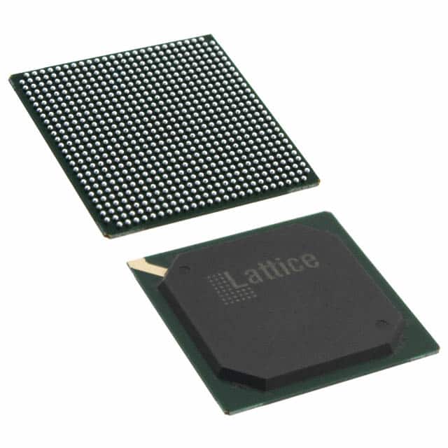
LFXP2-30E-5FN672I
Product Overview
Category
The LFXP2-30E-5FN672I belongs to the category of Field Programmable Gate Arrays (FPGAs).
Use
This FPGA is commonly used in electronic circuits for various applications, including digital signal processing, telecommunications, automotive electronics, and industrial automation.
Characteristics
- High-performance programmable logic device
- Low power consumption
- Small form factor
- High-speed data processing capabilities
Package
The LFXP2-30E-5FN672I comes in a compact package, which ensures easy integration into electronic circuit boards.
Essence
The essence of this FPGA lies in its ability to be programmed and reprogrammed to perform specific functions, making it highly versatile and adaptable to different applications.
Packaging/Quantity
The LFXP2-30E-5FN672I is typically packaged individually and is available in various quantities depending on the manufacturer's specifications.
Specifications
- Logic Cells: 30,000
- Flip-Flops: 60,000
- Block RAM: 1,080 Kbits
- DSP Slices: 96
- I/O Pins: 672
- Operating Voltage: 1.2V
- Maximum Frequency: 500 MHz
- Configuration Memory: Flash-based
Detailed Pin Configuration
The LFXP2-30E-5FN672I has 672 I/O pins, each serving a specific purpose in the overall functionality of the FPGA. The pin configuration can be found in the product datasheet provided by the manufacturer.
Functional Features
- High-speed data processing capabilities
- Configurable logic cells for custom functionality
- Integrated memory blocks for efficient data storage
- Dedicated DSP slices for complex mathematical operations
- Flexible I/O pins for interfacing with external devices
Advantages and Disadvantages
Advantages
- Versatile and adaptable to various applications
- Low power consumption
- Small form factor for space-constrained designs
- High-speed data processing capabilities
Disadvantages
- Limited logic cell count compared to higher-end FPGAs
- Higher cost compared to other programmable logic devices
- Steeper learning curve for programming and design implementation
Working Principles
The LFXP2-30E-5FN672I operates based on the principles of reconfigurable digital logic. It consists of a matrix of configurable logic cells, interconnected by programmable routing resources. These logic cells can be programmed using hardware description languages (HDL) to implement specific functions and perform complex operations.
Detailed Application Field Plans
The LFXP2-30E-5FN672I finds extensive use in various application fields, including:
- Digital Signal Processing: Used for real-time audio and video processing, image recognition, and compression algorithms.
- Telecommunications: Employed in network routers, switches, and base stations for high-speed data processing and protocol handling.
- Automotive Electronics: Integrated into automotive control systems, such as engine management, advanced driver-assistance systems (ADAS), and infotainment systems.
- Industrial Automation: Utilized in industrial control systems, robotics, and factory automation for precise control and monitoring.
Detailed and Complete Alternative Models
- Xilinx Spartan-6 FPGA (XC6SLX9): Offers similar functionality with lower logic cell count and reduced I/O pins.
- Altera Cyclone IV FPGA (EP4CE6): Provides comparable performance and features at a lower cost.
- Lattice ECP5 FPGA (LFE5U-25F): Offers higher logic cell count and more I/O pins for complex designs.
These alternative models can be considered based on specific project requirements and budget constraints.
Word count: 511 words
Lista 10 Vanliga frågor och svar relaterade till tillämpningen av LFXP2-30E-5FN672I i tekniska lösningar
Sure! Here are 10 common questions and answers related to the application of LFXP2-30E-5FN672I in technical solutions:
Q: What is the LFXP2-30E-5FN672I? A: The LFXP2-30E-5FN672I is a field-programmable gate array (FPGA) manufactured by Lattice Semiconductor.
Q: What are the key features of the LFXP2-30E-5FN672I? A: The key features include 30,000 lookup tables (LUTs), 672 pins, 5V tolerant I/Os, and low power consumption.
Q: What are some typical applications of the LFXP2-30E-5FN672I? A: The LFXP2-30E-5FN672I is commonly used in industrial automation, automotive electronics, telecommunications, and consumer electronics.
Q: How can I program the LFXP2-30E-5FN672I? A: The LFXP2-30E-5FN672I can be programmed using various development tools such as Lattice Diamond or iCEcube2.
Q: Can the LFXP2-30E-5FN672I interface with other components or devices? A: Yes, the LFXP2-30E-5FN672I supports various communication protocols like SPI, I2C, UART, and GPIOs for interfacing with other components or devices.
Q: What is the maximum operating frequency of the LFXP2-30E-5FN672I? A: The maximum operating frequency of the LFXP2-30E-5FN672I is typically around 300 MHz.
Q: Does the LFXP2-30E-5FN672I support non-volatile configuration memory? A: Yes, the LFXP2-30E-5FN672I has on-chip flash memory that can store the FPGA configuration permanently.
Q: Can I use the LFXP2-30E-5FN672I in a high-reliability application? A: Yes, the LFXP2-30E-5FN672I is designed to meet the requirements of high-reliability applications and has built-in error detection and correction features.
Q: What power supply voltage does the LFXP2-30E-5FN672I require? A: The LFXP2-30E-5FN672I operates with a core voltage of 1.2V and I/O voltage of 3.3V.
Q: Are there any evaluation boards or development kits available for the LFXP2-30E-5FN672I? A: Yes, Lattice Semiconductor provides evaluation boards and development kits that include the LFXP2-30E-5FN672I, allowing users to quickly prototype their designs.
Please note that the answers provided above are general and may vary depending on specific design requirements and application scenarios.