

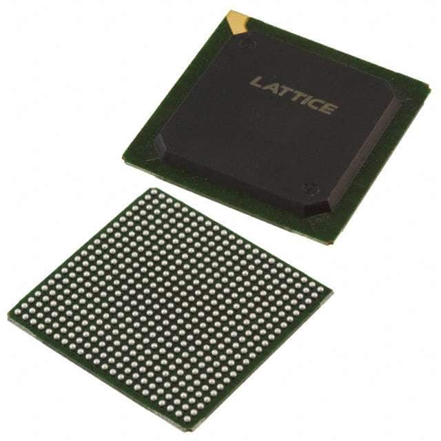
LFEC33E-4F484C
Product Overview
Category
LFEC33E-4F484C belongs to the category of Field-Programmable Gate Arrays (FPGAs).
Use
This product is primarily used in digital logic circuits for various applications such as telecommunications, automotive, industrial automation, and consumer electronics.
Characteristics
- High-performance FPGA with advanced features
- Low power consumption
- Flexible and reconfigurable design
- High-speed data processing capabilities
Package
The LFEC33E-4F484C comes in a compact package that ensures easy integration into electronic systems. It is designed to be mounted on a printed circuit board (PCB) using surface mount technology (SMT).
Essence
The essence of LFEC33E-4F484C lies in its ability to provide a customizable and programmable logic solution for complex digital designs.
Packaging/Quantity
Each LFEC33E-4F484C unit is packaged individually and is available in standard quantities of 1,000 units per reel.
Specifications
- Logic Elements: 33,000
- Flip-Flops: 66,000
- Block RAM: 1,080 Kbits
- Maximum Frequency: 500 MHz
- I/O Pins: 484
- Voltage Range: 1.2V - 3.3V
- Operating Temperature: -40°C to +85°C
Detailed Pin Configuration
The LFEC33E-4F484C has a well-defined pin configuration that facilitates easy integration into electronic systems. The detailed pin configuration can be found in the product datasheet.
Functional Features
- High-density programmable logic elements for complex designs
- Dedicated high-speed input/output (I/O) pins for efficient data transfer
- Built-in memory blocks for data storage and retrieval
- Clock management resources for precise timing control
- Flexible routing architecture for customizable interconnections
Advantages and Disadvantages
Advantages
- Versatile and adaptable to various applications
- High-performance capabilities for demanding tasks
- Low power consumption for energy-efficient designs
- Reconfigurable design allows for easy updates and modifications
Disadvantages
- Steep learning curve for beginners due to complex programming requirements
- Relatively higher cost compared to traditional fixed-function integrated circuits
- Limited availability of alternative models with similar specifications
Working Principles
The LFEC33E-4F484C operates based on the principles of field-programmable gate arrays. It consists of a matrix of configurable logic blocks interconnected through programmable routing resources. The device can be programmed using hardware description languages (HDL) or specialized software tools to implement desired digital logic functions.
Detailed Application Field Plans
The LFEC33E-4F484C finds extensive application in various fields, including:
- Telecommunications: Used in network routers, switches, and base stations for high-speed data processing and protocol handling.
- Automotive: Employed in automotive electronics for engine control units, advanced driver-assistance systems (ADAS), and infotainment systems.
- Industrial Automation: Utilized in programmable logic controllers (PLCs), motor control systems, and industrial robots for precise control and automation.
- Consumer Electronics: Integrated into smart TVs, gaming consoles, and home automation systems for enhanced functionality and performance.
Detailed and Complete Alternative Models
While the LFEC33E-4F484C offers a comprehensive set of features, there are alternative models available in the market that cater to different requirements. Some notable alternatives include:
- Xilinx Virtex UltraScale+ FPGA
- Intel Stratix 10 FPGA
- Lattice ECP5 FPGA
- Microchip PolarFire FPGA
These alternative models provide a range of options in terms of logic capacity, I/O capabilities, power consumption, and cost, allowing designers to choose the most suitable FPGA for their specific application needs.
In conclusion, the LFEC33E-4F484C is a high-performance FPGA that offers flexibility, reconfigurability, and advanced features. It finds applications in various fields and provides designers with a customizable logic solution for complex digital designs.
Lista 10 Vanliga frågor och svar relaterade till tillämpningen av LFEC33E-4F484C i tekniska lösningar
Sure! Here are 10 common questions and answers related to the application of LFEC33E-4F484C in technical solutions:
Q: What is LFEC33E-4F484C? A: LFEC33E-4F484C is a specific model number of a field-programmable gate array (FPGA) manufactured by a company called Lattice Semiconductor.
Q: What is an FPGA? A: FPGA stands for Field-Programmable Gate Array. It is a type of integrated circuit that can be programmed after manufacturing to perform specific functions.
Q: What are the key features of LFEC33E-4F484C? A: Some key features of LFEC33E-4F484C include 33,280 logic cells, 1,620 Kbits of embedded memory, 96 DSP blocks, and support for various I/O standards.
Q: In what applications can LFEC33E-4F484C be used? A: LFEC33E-4F484C can be used in a wide range of applications such as industrial automation, automotive electronics, telecommunications, medical devices, and more.
Q: How can LFEC33E-4F484C be programmed? A: LFEC33E-4F484C can be programmed using hardware description languages (HDLs) like VHDL or Verilog, or through graphical programming tools provided by Lattice Semiconductor.
Q: Can LFEC33E-4F484C be reprogrammed multiple times? A: Yes, LFEC33E-4F484C is a reprogrammable FPGA, which means it can be reprogrammed multiple times to implement different functionalities.
Q: What kind of development tools are available for LFEC33E-4F484C? A: Lattice Semiconductor provides a suite of development tools, including software design tools, simulation tools, and programming cables, to facilitate the development process.
Q: What is the power consumption of LFEC33E-4F484C? A: The power consumption of LFEC33E-4F484C depends on the specific design and usage scenario. It is recommended to refer to the datasheet or consult Lattice Semiconductor for detailed power specifications.
Q: Can LFEC33E-4F484C interface with other electronic components? A: Yes, LFEC33E-4F484C supports various I/O standards and can interface with other electronic components such as sensors, actuators, memory devices, communication interfaces, and more.
Q: Are there any limitations or considerations when using LFEC33E-4F484C? A: Some considerations include understanding the FPGA's resource limitations, managing power consumption, ensuring proper signal integrity, and following best practices for FPGA design to achieve optimal performance.
Please note that the answers provided here are general and may vary depending on specific requirements and use cases.