

LFE3-35EA-7FN672I
Product Overview
Category
The LFE3-35EA-7FN672I belongs to the category of Field Programmable Gate Arrays (FPGAs).
Use
This FPGA is commonly used in various electronic devices and systems for digital logic implementation, such as communication equipment, industrial control systems, and consumer electronics.
Characteristics
- High-performance programmable logic device
- Offers flexibility and reconfigurability
- Provides a wide range of logic elements, memory blocks, and I/O interfaces
- Supports complex digital designs and algorithms
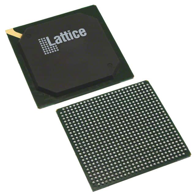
Package
The LFE3-35EA-7FN672I comes in a compact and durable package, ensuring easy integration into electronic circuits.
Essence
The essence of this FPGA lies in its ability to provide a customizable hardware platform that can be programmed to perform specific functions according to the user's requirements.
Packaging/Quantity
Each package of LFE3-35EA-7FN672I contains one unit of the FPGA.
Specifications
- Logic Elements: 33,280
- Embedded Memory: 1,152 Kbits
- Maximum Number of User I/Os: 520
- Clock Management Tiles: 8
- Maximum User Flash Memory: 2,048 Kbits
- Operating Voltage: 1.2V
- Speed Grade: -7
- Package Type: FineLine BGA
- Package Pins: 672
Detailed Pin Configuration
For a detailed pin configuration diagram of the LFE3-35EA-7FN672I, please refer to the manufacturer's datasheet or documentation.
Functional Features
- High-speed data processing capabilities
- Configurable I/O standards and voltage levels
- Built-in clock management resources
- Support for various communication protocols
- On-chip memory blocks for efficient data storage and retrieval
Advantages and Disadvantages
Advantages
- Flexibility to adapt to changing design requirements
- Faster time-to-market due to reprogrammability
- Lower development costs compared to custom ASICs
- High-performance computing capabilities
- Integration of multiple functions into a single device
Disadvantages
- Higher power consumption compared to dedicated hardware solutions
- Limited resources for complex designs
- Steeper learning curve for programming and utilization
Working Principles
The LFE3-35EA-7FN672I operates based on the principles of digital logic. It consists of configurable logic blocks, interconnects, and I/O interfaces. The user programs the FPGA using a Hardware Description Language (HDL) or a graphical design tool. Once programmed, the FPGA executes the desired logic functions by routing signals through its internal resources.
Detailed Application Field Plans
The LFE3-35EA-7FN672I finds applications in various fields, including:
- Communication Equipment: Used in routers, switches, and network infrastructure devices for high-speed data processing and protocol handling.
- Industrial Control Systems: Employed in automation systems, robotics, and manufacturing equipment for real-time control and monitoring.
- Consumer Electronics: Integrated into smart TVs, gaming consoles, and multimedia devices for enhanced performance and functionality.
Detailed and Complete Alternative Models
- LFE3-17EA-6FN484C: A lower-cost alternative with reduced logic elements and I/O count.
- LFE5UM-85F-8MG756C: A higher-end model with increased logic capacity and advanced features.
- LCMXO2-1200ZE-1TG144C: A smaller-sized FPGA suitable for low-power applications.
Please note that the above list is not exhaustive, and there are several other alternative models available in the market.
Word Count: 511
Lista 10 Vanliga frågor och svar relaterade till tillämpningen av LFE3-35EA-7FN672I i tekniska lösningar
Sure! Here are 10 common questions and answers related to the application of LFE3-35EA-7FN672I in technical solutions:
Q: What is the LFE3-35EA-7FN672I? A: The LFE3-35EA-7FN672I is a specific model of Field-Programmable Gate Array (FPGA) manufactured by Lattice Semiconductor.
Q: What are the key features of the LFE3-35EA-7FN672I? A: Some key features include 35,000 Look-Up Tables (LUTs), 672-pin FineLine BGA package, high-speed I/O interfaces, and low power consumption.
Q: What are the typical applications of the LFE3-35EA-7FN672I? A: The LFE3-35EA-7FN672I is commonly used in various technical solutions such as telecommunications, industrial automation, automotive electronics, and medical devices.
Q: How can I program the LFE3-35EA-7FN672I? A: The LFE3-35EA-7FN672I can be programmed using industry-standard Hardware Description Languages (HDLs) like VHDL or Verilog, along with specialized software tools provided by Lattice Semiconductor.
Q: What are the advantages of using the LFE3-35EA-7FN672I in my design? A: The LFE3-35EA-7FN672I offers flexibility, reconfigurability, and high-performance capabilities, allowing for rapid prototyping, customization, and optimization of complex digital systems.
Q: Can the LFE3-35EA-7FN672I interface with other components or devices? A: Yes, the LFE3-35EA-7FN672I supports various communication protocols such as SPI, I2C, UART, and Ethernet, enabling seamless integration with other components or devices in your design.
Q: What is the power consumption of the LFE3-35EA-7FN672I? A: The LFE3-35EA-7FN672I is designed to be power-efficient, consuming low power during normal operation. The exact power consumption depends on the specific implementation and usage scenario.
Q: Can the LFE3-35EA-7FN672I handle high-speed data processing? A: Yes, the LFE3-35EA-7FN672I is capable of handling high-speed data processing due to its advanced architecture and support for high-speed I/O interfaces like LVDS and DDR3/DDR4 memory.
Q: Are there any development boards or evaluation kits available for the LFE3-35EA-7FN672I? A: Yes, Lattice Semiconductor provides development boards and evaluation kits specifically designed for the LFE3-35EA-7FN672I, allowing users to quickly prototype and test their designs.
Q: Where can I find technical documentation and support for the LFE3-35EA-7FN672I? A: Technical documentation, datasheets, application notes, and support resources for the LFE3-35EA-7FN672I can be found on the official website of Lattice Semiconductor or by contacting their customer support team.
Please note that the answers provided here are general and may vary depending on specific requirements and use cases.