

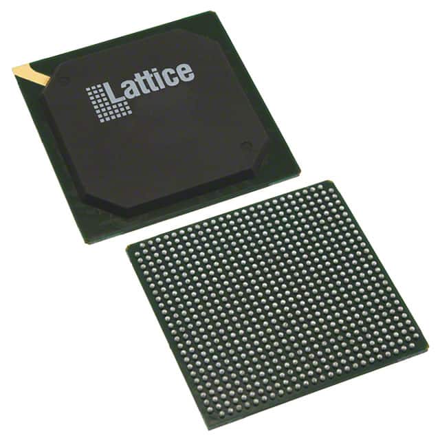
LFE3-150EA-8FN672I
Product Overview
Category
The LFE3-150EA-8FN672I belongs to the category of Field Programmable Gate Arrays (FPGAs).
Use
FPGAs are integrated circuits that can be programmed and reprogrammed to perform various digital functions. The LFE3-150EA-8FN672I is specifically designed for high-performance applications.
Characteristics
- High-performance FPGA with advanced features
- Flexible and programmable design
- Offers a wide range of logic elements, memory blocks, and I/O interfaces
- Supports complex digital designs and algorithms
Package
The LFE3-150EA-8FN672I comes in a compact and durable package suitable for electronic circuit integration.
Essence
The essence of the LFE3-150EA-8FN672I lies in its ability to provide a customizable and high-performance solution for digital circuit implementation.
Packaging/Quantity
The LFE3-150EA-8FN672I is typically packaged individually and is available in various quantities depending on the requirements of the user.
Specifications
- FPGA Family: LatticeECP3
- Logic Cells: 149,760
- Embedded Memory: 4,608 Kbits
- Maximum Number of I/Os: 622
- Operating Voltage: 1.2V
- Package Type: FBGA
- Package Pins: 672
- Speed Grade: -8
Detailed Pin Configuration
For a detailed pin configuration diagram of the LFE3-150EA-8FN672I, please refer to the manufacturer's datasheet or technical documentation.
Functional Features
- High-speed performance with low power consumption
- Configurable logic elements for implementing complex digital designs
- Built-in memory blocks for efficient data storage and retrieval
- Support for various communication protocols and interfaces
- Flexible clock management and synchronization capabilities
Advantages and Disadvantages
Advantages
- High-performance FPGA suitable for demanding applications
- Flexibility to adapt to changing design requirements
- Efficient utilization of resources with advanced optimization techniques
- Wide range of I/O options for interfacing with external devices
Disadvantages
- Steep learning curve for beginners due to the complexity of FPGA programming
- Higher cost compared to other programmable logic devices
- Limited availability of alternative models with similar specifications
Working Principles
The LFE3-150EA-8FN672I operates based on the principles of reconfigurable digital logic. It consists of a matrix of configurable logic elements interconnected through programmable routing resources. The user can program the FPGA to implement desired digital functions by configuring the logic elements and interconnections.
Detailed Application Field Plans
The LFE3-150EA-8FN672I finds applications in various fields, including: - Telecommunications and networking equipment - Industrial automation and control systems - High-performance computing - Aerospace and defense systems - Medical imaging and diagnostics - Video and image processing
Detailed and Complete Alternative Models
While the LFE3-150EA-8FN672I offers unique features and specifications, there are alternative FPGA models available from different manufacturers. Some notable alternatives include: - Xilinx Virtex UltraScale+ - Intel Stratix 10 - Microsemi PolarFire
These alternative models provide similar functionality and performance, allowing users to choose the most suitable FPGA for their specific application requirements.
Word count: 446 words
Lista 10 Vanliga frågor och svar relaterade till tillämpningen av LFE3-150EA-8FN672I i tekniska lösningar
Sure! Here are 10 common questions and answers related to the application of LFE3-150EA-8FN672I in technical solutions:
Q: What is the LFE3-150EA-8FN672I? A: The LFE3-150EA-8FN672I is a field-programmable gate array (FPGA) manufactured by Lattice Semiconductor.
Q: What are the key features of the LFE3-150EA-8FN672I? A: The key features include 150,000 lookup tables (LUTs), high-speed I/O interfaces, embedded memory blocks, and low power consumption.
Q: In what applications can the LFE3-150EA-8FN672I be used? A: The LFE3-150EA-8FN672I can be used in various applications such as telecommunications, industrial automation, automotive electronics, and medical devices.
Q: How can I program the LFE3-150EA-8FN672I? A: The LFE3-150EA-8FN672I can be programmed using hardware description languages (HDL) like VHDL or Verilog, or through graphical programming tools provided by Lattice Semiconductor.
Q: What are the advantages of using the LFE3-150EA-8FN672I in my design? A: The advantages include its flexibility, reconfigurability, high performance, and ability to handle complex logic functions.
Q: Can the LFE3-150EA-8FN672I interface with other components or devices? A: Yes, the LFE3-150EA-8FN672I supports various communication protocols such as SPI, I2C, UART, and Ethernet, allowing it to interface with other components or devices.
Q: What is the power consumption of the LFE3-150EA-8FN672I? A: The power consumption depends on the specific design and usage, but the LFE3-150EA-8FN672I is known for its low power characteristics.
Q: Can I use the LFE3-150EA-8FN672I for real-time signal processing? A: Yes, the LFE3-150EA-8FN672I is capable of handling real-time signal processing tasks due to its high-speed I/O interfaces and computational capabilities.
Q: Are there any development tools available for designing with the LFE3-150EA-8FN672I? A: Yes, Lattice Semiconductor provides a suite of development tools, including software IDEs, simulation tools, and debugging utilities, to aid in the design process.
Q: Where can I find more information about the LFE3-150EA-8FN672I? A: You can find more detailed information, datasheets, application notes, and reference designs on the official website of Lattice Semiconductor or by contacting their technical support team.
Please note that the answers provided here are general and may vary depending on specific requirements and use cases.