

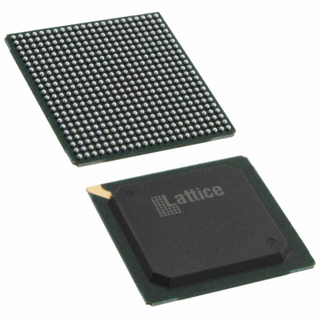
LFE2M50SE-7F484C
Product Overview
Category
The LFE2M50SE-7F484C belongs to the category of Field Programmable Gate Arrays (FPGAs).
Use
FPGAs are integrated circuits that can be programmed and reprogrammed to perform various digital functions. The LFE2M50SE-7F484C is specifically designed for applications requiring high-performance and low-power consumption.
Characteristics
- High performance: The LFE2M50SE-7F484C offers a large number of logic elements and built-in memory blocks, enabling complex digital designs.
- Low power consumption: This FPGA utilizes advanced power management techniques, making it suitable for battery-powered devices.
- Flexible configuration: The LFE2M50SE-7F484C allows users to customize the circuitry according to their specific requirements.
Package
The LFE2M50SE-7F484C comes in a 484-pin FineLine BGA package.
Essence
The essence of the LFE2M50SE-7F484C lies in its ability to provide a highly configurable and programmable platform for digital circuit design.
Packaging/Quantity
The LFE2M50SE-7F484C is typically sold individually or in reels, with the quantity varying based on customer requirements.
Specifications
- Logic Elements: 50,000
- Memory Blocks: 1,728 Kbits
- Maximum Frequency: 400 MHz
- I/O Pins: 316
- Operating Voltage: 1.2V
- Package Type: FineLine BGA
- Temperature Range: -40°C to +100°C
Detailed Pin Configuration
The LFE2M50SE-7F484C has a total of 484 pins, each serving a specific purpose in the circuit design. The pin configuration includes input/output pins, power supply pins, clock pins, and configuration pins. For a detailed pin configuration diagram, please refer to the manufacturer's datasheet.
Functional Features
- High-speed performance: The LFE2M50SE-7F484C offers fast signal processing capabilities, making it suitable for applications requiring real-time data processing.
- Low power consumption: This FPGA incorporates power-saving techniques, enabling energy-efficient operation.
- Flexible I/O options: The device provides a wide range of I/O standards, allowing seamless integration with various external devices.
- Embedded memory blocks: The LFE2M50SE-7F484C includes a significant amount of on-chip memory, facilitating efficient data storage and retrieval.
Advantages and Disadvantages
Advantages
- Versatility: The LFE2M50SE-7F484C can be programmed to perform a wide range of functions, making it adaptable to diverse application requirements.
- High-performance capabilities: With its large number of logic elements and high operating frequency, this FPGA can handle complex digital designs efficiently.
- Low-power operation: The LFE2M50SE-7F484C consumes minimal power, making it suitable for battery-powered devices.
Disadvantages
- Complexity: Programming and configuring FPGAs can be challenging for beginners due to their inherent complexity.
- Cost: FPGAs, including the LFE2M50SE-7F484C, tend to be more expensive compared to other integrated circuits.
Working Principles
The LFE2M50SE-7F484C operates based on the principles of reconfigurable computing. It consists of an array of configurable logic blocks interconnected through programmable routing resources. These logic blocks can be programmed to implement desired digital functions by configuring the interconnections and functionality of the individual blocks.
Detailed Application Field Plans
The LFE2M50SE-7F484C finds applications in various fields, including:
- Communications: It can be used in wireless communication systems for signal processing and protocol implementation.
- Industrial Automation: The FPGA can be employed in control systems, motor drives, and robotics to enable precise and flexible automation.
- Image and Video Processing: The LFE2M50SE-7F484C is suitable for real-time image and video processing tasks, such as object recognition and video compression.
- Aerospace and Defense: It can be utilized in radar systems, avionics, and military-grade communication equipment.
Detailed and Complete Alternative Models
- LFE2M35SE-5F672C: A similar FPGA with a lower logic element count but offering cost advantages.
- LFE2M100SE-7FN1152C: A higher-end FPGA with increased logic elements and memory blocks, suitable for more complex designs.
- LFE2M20SE-6F256C: A smaller-sized FPGA with reduced power consumption, ideal for space-constrained applications.
These alternative models provide options based on varying requirements and constraints
Lista 10 Vanliga frågor och svar relaterade till tillämpningen av LFE2M50SE-7F484C i tekniska lösningar
Sure! Here are 10 common questions and answers related to the application of LFE2M50SE-7F484C in technical solutions:
Q: What is the LFE2M50SE-7F484C? A: The LFE2M50SE-7F484C is a specific model of Field-Programmable Gate Array (FPGA) manufactured by Lattice Semiconductor.
Q: What are the key features of the LFE2M50SE-7F484C? A: Some key features of this FPGA include 50,000 Look-Up Tables (LUTs), 1,152 Kbits of embedded memory, 184 user I/O pins, and support for various communication protocols.
Q: What are the typical applications of the LFE2M50SE-7F484C? A: This FPGA is commonly used in applications such as industrial automation, telecommunications, automotive electronics, medical devices, and aerospace systems.
Q: How can I program the LFE2M50SE-7F484C? A: The LFE2M50SE-7F484C can be programmed using the Lattice Diamond design software or other compatible programming tools provided by Lattice Semiconductor.
Q: What voltage levels does the LFE2M50SE-7F484C support? A: This FPGA supports various voltage levels, including 1.2V core voltage and 3.3V or 2.5V I/O voltage options.
Q: Can I interface the LFE2M50SE-7F484C with other components or microcontrollers? A: Yes, the LFE2M50SE-7F484C provides multiple I/O pins that can be used to interface with other components or microcontrollers in your system.
Q: Does the LFE2M50SE-7F484C support high-speed serial communication protocols? A: Yes, this FPGA supports various high-speed serial communication protocols such as PCIe, Gigabit Ethernet, and USB.
Q: Can I reprogram the LFE2M50SE-7F484C after it has been deployed in a system? A: Yes, the LFE2M50SE-7F484C is a field-programmable device, which means you can reprogram it even after it has been soldered onto a PCB.
Q: Are there any development boards available for the LFE2M50SE-7F484C? A: Yes, Lattice Semiconductor provides development boards specifically designed for the LFE2M50SE-7F484C, which can help you prototype and test your designs.
Q: Where can I find more technical documentation and support for the LFE2M50SE-7F484C? A: You can find detailed technical documentation, datasheets, application notes, and support resources on the official website of Lattice Semiconductor or by contacting their customer support team.
Please note that the answers provided here are general and may vary depending on specific requirements and use cases. It's always recommended to refer to the official documentation and consult with experts when working with specific technical solutions.