

LFE2M50SE-6F900I
Product Overview
Category
The LFE2M50SE-6F900I belongs to the category of Field Programmable Gate Arrays (FPGAs).
Use
This FPGA is designed for various applications that require high-performance and flexible digital logic circuits.
Characteristics
- High-performance digital logic circuit implementation
- Flexibility in reprogramming and customization
- Low power consumption
- Compact package size
- Wide operating temperature range
Package
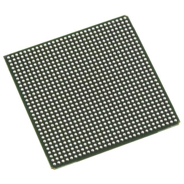
The LFE2M50SE-6F900I comes in a compact package, suitable for surface mount technology (SMT) assembly.
Essence
The essence of this FPGA lies in its ability to implement complex digital logic circuits with high performance and flexibility.
Packaging/Quantity
The LFE2M50SE-6F900I is typically packaged in reels or trays, containing a specific quantity per package. Please refer to the manufacturer's specifications for detailed packaging information.
Specifications
- Model: LFE2M50SE-6F900I
- Logic Elements: 50,000
- Speed Grade: -6
- Operating Voltage: 3.3V
- I/O Pins: 900
- Memory Blocks: 1,800
- Maximum Frequency: 900 MHz
- Package Type: SE (Small Edge)
- Package Size: 17mm x 17mm
Detailed Pin Configuration
The LFE2M50SE-6F900I has a total of 900 I/O pins, which are configurable for various purposes. The pin configuration can be found in the manufacturer's datasheet.
Functional Features
- High-speed data processing capabilities
- Configurable I/O pins for versatile connectivity options
- On-chip memory blocks for efficient data storage
- Built-in clock management resources for precise timing control
- Support for various communication protocols and interfaces
- Flexible routing resources for complex interconnections
Advantages and Disadvantages
Advantages
- High-performance digital logic implementation
- Flexibility in reprogramming and customization
- Low power consumption compared to traditional ASICs
- Compact package size allows for space-efficient designs
- Wide operating temperature range enables usage in various environments
Disadvantages
- Steeper learning curve compared to standard microcontrollers
- Higher cost compared to off-the-shelf microcontrollers for simple applications
- Limited availability of specialized technical support compared to mainstream microcontrollers
Working Principles
The LFE2M50SE-6F900I operates based on the principles of field-programmable gate arrays. It consists of configurable logic elements, memory blocks, I/O pins, and other resources that can be programmed to implement desired digital logic circuits. The FPGA is programmed using a hardware description language (HDL) or a graphical design tool, which configures the internal resources to achieve the desired functionality.
Detailed Application Field Plans
The LFE2M50SE-6F900I finds applications in various fields, including but not limited to: - Telecommunications - Data processing and storage systems - Industrial automation - Medical devices - Aerospace and defense - Automotive electronics
In telecommunications, this FPGA can be used for high-speed data packet processing, protocol conversion, and signal modulation/demodulation. In industrial automation, it can enable real-time control and monitoring of complex systems. In medical devices, it can facilitate image processing, signal analysis, and patient monitoring. In aerospace and defense, it can be utilized for radar signal processing, encryption/decryption, and mission-critical control systems. In automotive electronics, it can enhance driver assistance systems, infotainment, and engine control.
Detailed and Complete Alternative Models
- LFE2M35SE-5F672I
- LFE2M100SE-7FN1152C
- LFE3-35EA-6FN484C
These alternative models offer different combinations of logic elements, I/O pins, speed grades, and package sizes to cater to specific application requirements. Please refer to the manufacturer's documentation for detailed specifications of each alternative model.
In conclusion, the LFE2M50SE-6F900I is a high-performance FPGA that provides flexibility, low power consumption, and compact packaging. Its functional features, advantages, and disadvantages make it suitable for various applications in telecommunications, data processing, industrial automation, medical devices, aerospace and defense, and automotive electronics. Additionally, there are alternative models available with varying specifications to meet specific application needs.
Lista 10 Vanliga frågor och svar relaterade till tillämpningen av LFE2M50SE-6F900I i tekniska lösningar
Sure! Here are 10 common questions and answers related to the application of LFE2M50SE-6F900I in technical solutions:
Q: What is the LFE2M50SE-6F900I? A: The LFE2M50SE-6F900I is a specific model of Field-Programmable Gate Array (FPGA) manufactured by Lattice Semiconductor.
Q: What are the key features of the LFE2M50SE-6F900I? A: Some key features of this FPGA include 50,000 logic elements, 900 MHz maximum operating frequency, and support for various I/O standards.
Q: In what technical solutions can the LFE2M50SE-6F900I be used? A: The LFE2M50SE-6F900I can be used in a wide range of applications such as industrial automation, telecommunications, automotive, medical devices, and more.
Q: How can I program the LFE2M50SE-6F900I? A: The LFE2M50SE-6F900I can be programmed using various design tools provided by Lattice Semiconductor, such as Lattice Diamond or Lattice Radiant.
Q: What programming languages are supported by the LFE2M50SE-6F900I? A: The LFE2M50SE-6F900I supports popular hardware description languages (HDLs) like VHDL and Verilog for designing and programming the FPGA.
Q: Can I use the LFE2M50SE-6F900I for high-speed data processing? A: Yes, the LFE2M50SE-6F900I's high operating frequency of 900 MHz makes it suitable for applications requiring high-speed data processing.
Q: Does the LFE2M50SE-6F900I support external memory interfaces? A: Yes, the LFE2M50SE-6F900I supports various memory interfaces like DDR3, DDR4, and LPDDR4, allowing for efficient data storage and retrieval.
Q: Can I interface the LFE2M50SE-6F900I with other electronic components or devices? A: Absolutely! The LFE2M50SE-6F900I offers a wide range of I/O standards, including LVCMOS, LVTTL, LVDS, and more, enabling easy integration with other components.
Q: What power supply requirements does the LFE2M50SE-6F900I have? A: The LFE2M50SE-6F900I typically operates at a voltage range of 1.14V to 1.26V, with additional power supply pins for I/O banks and configuration.
Q: Where can I find more information about the LFE2M50SE-6F900I? A: You can find detailed technical documentation, datasheets, and application notes on the official website of Lattice Semiconductor or by contacting their support team.
Please note that the answers provided here are general and may vary depending on specific requirements and use cases.