

LFE2M20SE-7FN484C
Product Overview
Category
The LFE2M20SE-7FN484C belongs to the category of Field Programmable Gate Arrays (FPGAs).
Use
This FPGA is commonly used in various electronic devices and systems for digital logic implementation, such as communication equipment, industrial control systems, and consumer electronics.
Characteristics
- High-performance programmable logic device
- Offers flexibility and reconfigurability
- Provides a large number of configurable logic blocks (CLBs) and programmable interconnects
- Supports complex digital designs and algorithms
- Enables rapid prototyping and development cycles
Package
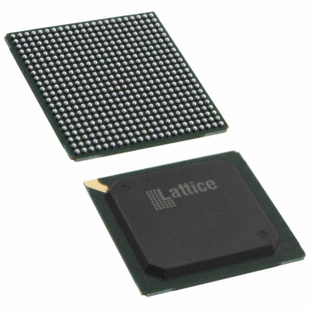
The LFE2M20SE-7FN484C comes in a 484-pin FineLine BGA (Ball Grid Array) package.
Essence
The essence of this FPGA lies in its ability to provide a customizable hardware platform that allows designers to implement complex digital circuits and algorithms efficiently.
Packaging/Quantity
The LFE2M20SE-7FN484C is typically packaged individually and is available in various quantities depending on the manufacturer or distributor.
Specifications
- Logic Elements: 19,200
- Embedded Memory: 504 Kbits
- Maximum User I/Os: 316
- Block RAM: 1,080 Kbits
- Clock Management Tiles: 8
- Maximum Distributed RAM: 1,152 Kbits
- Maximum PLLs: 4
- Maximum Global Clocks: 16
Detailed Pin Configuration
The LFE2M20SE-7FN484C has a total of 484 pins. The pin configuration includes input/output pins, power supply pins, ground pins, and configuration pins. For a detailed pin configuration diagram, please refer to the datasheet provided by the manufacturer.
Functional Features
- High-speed performance with low power consumption
- Configurable I/O standards and voltage levels
- Built-in clock management resources for precise timing control
- On-chip memory blocks for efficient data storage
- Flexible routing architecture for interconnecting various components
- Support for multiple communication protocols
Advantages and Disadvantages
Advantages
- Flexibility and reconfigurability allow for rapid prototyping and design iterations
- High-performance capabilities enable the implementation of complex digital designs
- Availability of a large number of logic elements and memory blocks
- Support for various I/O standards and voltage levels
- Cost-effective solution compared to custom ASIC (Application-Specific Integrated Circuit) designs
Disadvantages
- Steeper learning curve compared to traditional fixed-function integrated circuits
- Limited performance compared to dedicated hardware implementations
- Higher power consumption compared to application-specific solutions
Working Principles
The LFE2M20SE-7FN484C operates based on the principles of field-programmable gate arrays. It consists of configurable logic blocks (CLBs), programmable interconnects, embedded memory blocks, and other supporting resources. The device can be programmed using hardware description languages (HDLs) such as VHDL or Verilog. Once programmed, the FPGA executes the desired digital logic functions by configuring its internal resources accordingly.
Detailed Application Field Plans
The LFE2M20SE-7FN484C finds applications in various fields, including:
- Communication Equipment: Used in networking devices, routers, and switches for high-speed data processing and protocol handling.
- Industrial Control Systems: Employed in automation systems, robotics, and process control applications for real-time control and monitoring.
- Consumer Electronics: Integrated into multimedia devices, gaming consoles, and smart appliances for enhanced functionality and performance.
Detailed and Complete Alternative Models
- LFE2M35SE-7FN484C: A higher-capacity FPGA with 35,200 logic elements and increased memory resources.
- LFE2M12SE-7FN484C: A lower-capacity FPGA with 12,800 logic elements, suitable for smaller-scale designs.
- LFE2M25SE-7FN484C: An intermediate-capacity FPGA with 25,600 logic elements, offering a balance between performance and cost.
These alternative models provide different capacity options to cater to varying design requirements.
Note: The above information is based on the specifications provided by the manufacturer and may vary depending on the specific version or revision of the product.
Lista 10 Vanliga frågor och svar relaterade till tillämpningen av LFE2M20SE-7FN484C i tekniska lösningar
Sure! Here are 10 common questions and answers related to the application of LFE2M20SE-7FN484C in technical solutions:
Q: What is the LFE2M20SE-7FN484C? A: The LFE2M20SE-7FN484C is a specific model of Field-Programmable Gate Array (FPGA) manufactured by Lattice Semiconductor.
Q: What are the key features of the LFE2M20SE-7FN484C? A: Some key features of this FPGA include 20,000 Look-Up Tables (LUTs), 1,080 kilobits of embedded memory, 184 user I/O pins, and support for various communication protocols.
Q: What are the typical applications of the LFE2M20SE-7FN484C? A: This FPGA can be used in a wide range of applications such as industrial automation, automotive electronics, telecommunications, medical devices, and more.
Q: How can I program the LFE2M20SE-7FN484C? A: The LFE2M20SE-7FN484C can be programmed using the Lattice Diamond design software or other compatible programming tools provided by Lattice Semiconductor.
Q: What voltage levels does the LFE2M20SE-7FN484C support? A: This FPGA supports both 3.3V and 1.2V voltage levels, making it compatible with a variety of digital systems.
Q: Can I interface the LFE2M20SE-7FN484C with external devices? A: Yes, the LFE2M20SE-7FN484C provides multiple I/O pins that can be used to interface with external devices such as sensors, actuators, displays, and more.
Q: Does the LFE2M20SE-7FN484C support any specific communication protocols? A: Yes, this FPGA supports various communication protocols such as SPI, I2C, UART, and GPIO, allowing for easy integration with other components in a system.
Q: What are the power requirements for the LFE2M20SE-7FN484C? A: The LFE2M20SE-7FN484C typically operates at a supply voltage of 3.3V, but it also has a separate 1.2V core voltage requirement.
Q: Can I use the LFE2M20SE-7FN484C in high-reliability applications? A: Yes, this FPGA is designed to meet certain industry standards for reliability, making it suitable for use in critical applications that require robust performance.
Q: Where can I find additional technical documentation and support for the LFE2M20SE-7FN484C? A: You can find detailed technical documentation, datasheets, application notes, and support resources on the official website of Lattice Semiconductor or by contacting their customer support team.
Please note that the answers provided here are general and may vary depending on specific requirements and use cases. It's always recommended to refer to the official documentation and consult with experts for accurate information.