

LFE2M100E-6F900I
Product Overview
Category
The LFE2M100E-6F900I belongs to the category of Field Programmable Gate Arrays (FPGAs).
Use
This FPGA is primarily used in electronic circuits for digital logic implementation, prototyping, and system integration.
Characteristics
- High-performance programmable logic device
- Offers flexibility and reconfigurability
- Enables rapid development and customization of digital circuits
- Supports complex designs and algorithms
- Provides high-speed data processing capabilities
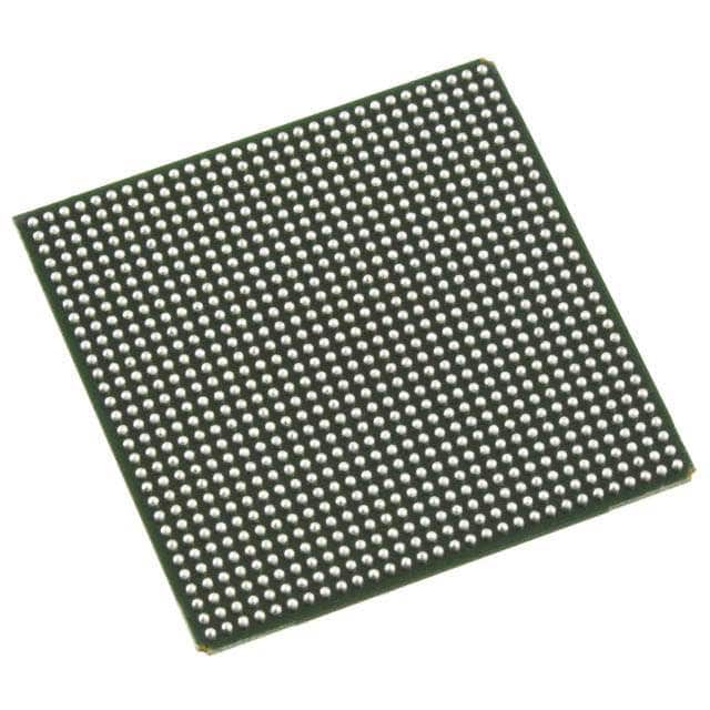
Package
The LFE2M100E-6F900I comes in a compact and durable package that ensures protection during handling and installation.
Essence
The essence of this FPGA lies in its ability to provide a versatile platform for implementing complex digital logic designs with high performance and flexibility.
Packaging/Quantity
The LFE2M100E-6F900I is typically packaged individually and is available in various quantities depending on the manufacturer's specifications.
Specifications
- Model: LFE2M100E-6F900I
- Logic Elements: 100,000
- Speed Grade: -6
- Operating Voltage: 3.3V
- I/O Pins: 900
- Memory Blocks: 4,800 Kbits
- Clock Management Tiles: 10
- DSP Blocks: 360
- Maximum Frequency: 900 MHz
- Package Type: FineLine BGA
Detailed Pin Configuration
The LFE2M100E-6F900I has a comprehensive pin configuration that includes various input/output pins, power supply pins, and configuration pins. For detailed pin configuration information, please refer to the manufacturer's datasheet.
Functional Features
- High-density programmable logic elements for complex designs
- Dedicated clock management tiles for precise timing control
- Integrated DSP blocks for efficient signal processing
- Flexible I/O pins for interfacing with external devices
- On-chip memory blocks for data storage and retrieval
Advantages and Disadvantages
Advantages
- Offers high performance and flexibility in digital circuit implementation
- Enables rapid prototyping and system integration
- Supports complex designs and algorithms
- Provides efficient signal processing capabilities
- Allows for reconfiguration and updates without hardware changes
Disadvantages
- Requires expertise in FPGA programming and design
- Higher cost compared to fixed-function integrated circuits
- Limited availability of alternative models with similar specifications
Working Principles
The LFE2M100E-6F900I operates based on the principles of field-programmable gate arrays. It consists of a matrix of programmable logic elements interconnected through configurable routing resources. These logic elements can be programmed to implement various digital functions, allowing for the creation of custom digital circuits.
Detailed Application Field Plans
The LFE2M100E-6F900I finds applications in a wide range of fields, including: 1. Telecommunications: Used in network infrastructure equipment for data processing and protocol handling. 2. Aerospace and Defense: Employed in radar systems, avionics, and communication systems for signal processing and control. 3. Industrial Automation: Utilized in control systems, robotics, and machine vision applications for real-time data processing and control. 4. Medical Devices: Integrated into medical imaging systems, patient monitoring devices, and laboratory equipment for data acquisition and processing. 5. Automotive: Used in advanced driver-assistance systems (ADAS), infotainment systems, and engine control units for enhanced functionality and performance.
Detailed and Complete Alternative Models
While the LFE2M100E-6F900I offers unique features and specifications, there are alternative models available from different manufacturers that provide similar functionality. Some notable alternatives include: - Xilinx Virtex UltraScale+ FPGA - Intel Stratix 10 FPGA - Microsemi SmartFusion2 FPGA
These alternative models offer comparable performance and flexibility, providing users with a range of options for their specific application requirements.
Word count: 511
Lista 10 Vanliga frågor och svar relaterade till tillämpningen av LFE2M100E-6F900I i tekniska lösningar
Sure! Here are 10 common questions and answers related to the application of LFE2M100E-6F900I in technical solutions:
Q: What is the LFE2M100E-6F900I? A: The LFE2M100E-6F900I is a specific model of Field-Programmable Gate Array (FPGA) manufactured by Lattice Semiconductor.
Q: What are the key features of the LFE2M100E-6F900I? A: The key features of this FPGA include 100,000 logic elements, 900 MHz maximum operating frequency, and support for various I/O standards.
Q: In what technical solutions can the LFE2M100E-6F900I be used? A: The LFE2M100E-6F900I can be used in a wide range of applications such as telecommunications, industrial automation, automotive electronics, and medical devices.
Q: How does the LFE2M100E-6F900I benefit technical solutions? A: This FPGA offers high-performance processing capabilities, flexibility for customization, and low power consumption, making it suitable for complex and demanding applications.
Q: Can the LFE2M100E-6F900I interface with other components or devices? A: Yes, the LFE2M100E-6F900I supports various communication protocols and interfaces like SPI, I2C, UART, Ethernet, and PCIe, allowing seamless integration with other components.
Q: Is programming required for using the LFE2M100E-6F900I? A: Yes, the LFE2M100E-6F900I needs to be programmed using Hardware Description Languages (HDL) like VHDL or Verilog to define its functionality.
Q: Can the LFE2M100E-6F900I be reprogrammed after deployment? A: Yes, this FPGA is field-programmable, meaning it can be reprogrammed even after being deployed in a technical solution, allowing for flexibility and updates.
Q: What development tools are available for working with the LFE2M100E-6F900I? A: Lattice Semiconductor provides software tools like Lattice Diamond or Lattice Radiant for designing, programming, and debugging the LFE2M100E-6F900I.
Q: Are there any limitations or considerations when using the LFE2M100E-6F900I? A: Some considerations include power supply requirements, thermal management, and ensuring proper signal integrity due to high-speed operation.
Q: Where can I find more information about the LFE2M100E-6F900I and its application in technical solutions? A: You can refer to the official documentation and datasheets provided by Lattice Semiconductor, as well as online forums and communities dedicated to FPGA development.