

LCMXO640E-3MN132I
Product Overview
Category: Programmable Logic Device (PLD)
Use: The LCMXO640E-3MN132I is a high-performance PLD designed for various digital logic applications. It offers flexibility and versatility in implementing complex logic functions.
Characteristics: - Low power consumption - High-speed performance - Small form factor - Easy programmability
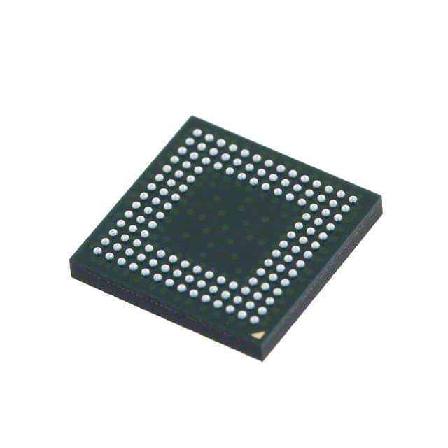
Package: The LCMXO640E-3MN132I comes in a compact 132-pin Quad Flat No-Lead (QFN) package, which ensures efficient heat dissipation and ease of integration into electronic systems.
Essence: This PLD is built to provide designers with a cost-effective solution for implementing custom logic functions in a wide range of applications.
Packaging/Quantity: The LCMXO640E-3MN132I is typically sold in reels or trays, with each reel containing a specific quantity of devices. Please refer to the manufacturer's specifications for detailed packaging and quantity information.
Specifications
- Logic Cells: 640
- I/O Pins: 132
- Operating Voltage: 1.2V
- Maximum Frequency: 300 MHz
- Programmable Logic Blocks: 40
- Embedded Memory: 64 Kbits
- Configuration Method: JTAG
Detailed Pin Configuration
The LCMXO640E-3MN132I features a total of 132 pins, each serving a specific purpose. The pin configuration is as follows:
(Pin Number) - (Pin Name) - (Function) 1 - VCCIO - Power supply for I/O banks 2 - GND - Ground reference 3 - IO0 - General-purpose I/O pin 0 4 - IO1 - General-purpose I/O pin 1 ... 132 - IO131 - General-purpose I/O pin 131
Please refer to the datasheet for a complete pin configuration table.
Functional Features
- High-speed performance: The LCMXO640E-3MN132I operates at a maximum frequency of 300 MHz, enabling rapid execution of complex logic functions.
- Low power consumption: This PLD is designed to minimize power consumption, making it suitable for battery-powered devices and energy-efficient applications.
- Flexible programmability: The device can be easily programmed using industry-standard tools, allowing designers to implement custom logic functions tailored to their specific requirements.
Advantages and Disadvantages
Advantages: - Cost-effective solution for implementing custom logic functions - Small form factor enables integration into space-constrained designs - Low power consumption extends battery life in portable devices - High-speed performance allows for efficient execution of complex logic functions
Disadvantages: - Limited number of logic cells compared to higher-end PLDs - May require additional external components for certain applications - Programming and debugging process may have a learning curve for beginners
Working Principles
The LCMXO640E-3MN132I utilizes a combination of configurable logic blocks, embedded memory, and interconnect resources to implement custom logic functions. It operates based on the principles of digital logic, where logical operations are performed using binary signals (0s and 1s).
The device can be programmed using hardware description languages (HDL) or schematic entry tools, which allow designers to define the desired logic functions and interconnections. Once programmed, the PLD executes the specified logic operations, providing the desired functionality.
Detailed Application Field Plans
The LCMXO640E-3MN132I finds applications in various fields, including but not limited to: - Industrial automation - Consumer electronics - Communications - Automotive systems - Medical devices
In industrial automation, this PLD can be used to implement control logic for machinery, process monitoring, and data acquisition systems. In consumer electronics, it can be utilized for audio/video processing, user interface control, and power management.
In the communications field, the LCMXO640E-3MN132I can be employed in network routers, switches, and wireless communication devices. Automotive systems can benefit from its use in engine control units (ECUs), driver assistance systems, and infotainment systems. Medical devices such as patient monitoring systems and diagnostic equipment can also utilize this PLD for custom logic implementation.
Detailed and Complete Alternative Models
- LCMXO256C-3TN100C
- LCMXO2-1200ZE-1TG144C
- LCMXO3LF-4300C-5BG256C
- LCMXO2280C-4FTN256C
These alternative models offer varying specifications and features, catering to different application requirements. Designers should evaluate their specific needs and consult the manufacturer's documentation for detailed information on each model.
Word count: 615 words
Lista 10 Vanliga frågor och svar relaterade till tillämpningen av LCMXO640E-3MN132I i tekniska lösningar
Sure! Here are 10 common questions and answers related to the application of LCMXO640E-3MN132I in technical solutions:
Q: What is the LCMXO640E-3MN132I? A: The LCMXO640E-3MN132I is a low-cost, low-power FPGA (Field-Programmable Gate Array) device manufactured by Lattice Semiconductor.
Q: What are the key features of the LCMXO640E-3MN132I? A: Some key features include 640 LUTs (Look-Up Tables), 32Kbits of embedded memory, 32 user I/O pins, and support for various I/O standards.
Q: What are some typical applications of the LCMXO640E-3MN132I? A: The LCMXO640E-3MN132I is commonly used in applications such as industrial control systems, consumer electronics, automotive systems, and IoT devices.
Q: How can I program the LCMXO640E-3MN132I? A: The LCMXO640E-3MN132I can be programmed using Lattice Diamond or Lattice Radiant software tools, which support various programming languages like VHDL and Verilog.
Q: What is the power consumption of the LCMXO640E-3MN132I? A: The LCMXO640E-3MN132I has a low power consumption, typically ranging from 10-100mW, depending on the design and operating conditions.
Q: Can I use the LCMXO640E-3MN132I in battery-powered devices? A: Yes, the low power consumption of the LCMXO640E-3MN132I makes it suitable for battery-powered devices, helping to extend the battery life.
Q: Does the LCMXO640E-3MN132I support communication interfaces? A: Yes, the LCMXO640E-3MN132I supports various communication interfaces such as SPI, I2C, UART, and GPIO, making it versatile for different applications.
Q: Can I use the LCMXO640E-3MN132I for real-time signal processing? A: Yes, the LCMXO640E-3MN132I can be used for real-time signal processing tasks by implementing algorithms in the FPGA fabric.
Q: Is the LCMXO640E-3MN132I suitable for high-speed applications? A: While the LCMXO640E-3MN132I is not specifically designed for high-speed applications, it can still handle moderate-speed designs depending on the specific requirements.
Q: Are there any development boards available for the LCMXO640E-3MN132I? A: Yes, Lattice Semiconductor provides development boards like the iCE40 UltraPlus Breakout Board, which can be used with the LCMXO640E-3MN132I for prototyping and evaluation purposes.
Please note that these answers are general and may vary based on specific design requirements and application scenarios.