

LCMXO3L-9400E-6BG484I
Product Overview
Category
The LCMXO3L-9400E-6BG484I belongs to the category of Field Programmable Gate Arrays (FPGAs).
Use
FPGAs are integrated circuits that can be programmed and reprogrammed to perform various digital functions. The LCMXO3L-9400E-6BG484I is specifically designed for applications requiring high-performance and low-power consumption.
Characteristics
- High performance: The LCMXO3L-9400E-6BG484I offers a combination of high-speed operation and low power consumption, making it suitable for demanding applications.
- Low power consumption: This FPGA is designed to minimize power usage, making it energy-efficient.
- Programmability: The LCMXO3L-9400E-6BG484I can be easily programmed and reprogrammed to adapt to different application requirements.
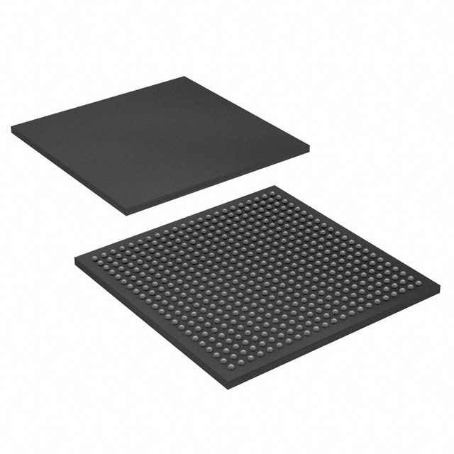
- Small package size: It comes in a compact 484-ball grid array (BGA) package, which allows for space-saving integration into electronic systems.
Package and Quantity
The LCMXO3L-9400E-6BG484I is packaged in a 484-ball BGA package. The quantity may vary depending on the supplier or customer requirements.
Specifications
- Logic Elements: 9400
- Look-Up Tables (LUTs): 4700
- Flip-Flops: 9400
- Block RAM: 270 Kbits
- Maximum Operating Frequency: Up to 300 MHz
- I/O Pins: 324
- Voltage Range: 1.2V - 3.3V
- Operating Temperature Range: -40°C to 85°C
Detailed Pin Configuration
The LCMXO3L-9400E-6BG484I has a total of 324 I/O pins. The pin configuration may vary depending on the specific application and design requirements. Please refer to the manufacturer's datasheet for detailed pin assignments.
Functional Features
- High-speed operation: The LCMXO3L-9400E-6BG484I offers fast processing capabilities, allowing for efficient execution of complex algorithms.
- Low power consumption: This FPGA is designed to minimize power usage, making it suitable for battery-powered devices or applications with strict power constraints.
- Flexible reprogrammability: The LCMXO3L-9400E-6BG484I can be easily reprogrammed to adapt to changing application requirements, providing flexibility in system design.
- Integrated peripherals: It supports various communication protocols and interfaces, enabling seamless integration with other electronic components.
Advantages and Disadvantages
Advantages
- High-performance capabilities
- Low power consumption
- Compact package size
- Flexible programmability
Disadvantages
- Limited logic elements compared to higher-end FPGAs
- May require additional external components for certain applications
Working Principles
The LCMXO3L-9400E-6BG484I operates based on the principles of digital logic. It consists of configurable logic blocks (CLBs), interconnects, and input/output (I/O) blocks. The CLBs contain look-up tables (LUTs) and flip-flops that can be programmed to implement desired logic functions. The interconnects provide routing paths between different CLBs and I/O blocks, enabling data flow within the FPGA. By configuring the CLBs and interconnects, users can create custom digital circuits tailored to their specific application requirements.
Detailed Application Field Plans
The LCMXO3L-9400E-6BG484I finds applications in various fields, including but not limited to:
- Communications: It can be used in wireless communication systems, network routers, and data transmission equipment.
- Industrial Automation: The FPGA's high-performance capabilities make it suitable for industrial control systems, robotics, and process automation.
- Automotive Electronics: It can be utilized in automotive control units, driver assistance systems, and infotainment systems.
- Medical Devices: The FPGA can be integrated into medical imaging equipment, patient monitoring systems, and diagnostic devices.
- Aerospace and Defense: It finds applications in radar systems, avionics, unmanned aerial vehicles (UAVs), and military communication systems.
Detailed and Complete Alternative Models
- LCMXO2-1200ZE-1TG144C
- LCMXO2-4000HE-6BG256C
- LCMXO2-7000HE-5TG144C
- LCMXO3L-6900E-6BG484I
- LCMXO3LF-4300E-5MG324C
These alternative models offer different specifications and features, providing options for
Lista 10 Vanliga frågor och svar relaterade till tillämpningen av LCMXO3L-9400E-6BG484I i tekniska lösningar
Sure! Here are 10 common questions and answers related to the application of LCMXO3L-9400E-6BG484I in technical solutions:
Q: What is the LCMXO3L-9400E-6BG484I? A: The LCMXO3L-9400E-6BG484I is a specific model of Field-Programmable Gate Array (FPGA) manufactured by Lattice Semiconductor.
Q: What are the key features of the LCMXO3L-9400E-6BG484I? A: Some key features include low power consumption, small form factor, high-performance logic fabric, and built-in I/O interfaces.
Q: What are the typical applications of LCMXO3L-9400E-6BG484I? A: This FPGA is commonly used in various technical solutions such as industrial automation, robotics, IoT devices, consumer electronics, and automotive systems.
Q: How can I program the LCMXO3L-9400E-6BG484I? A: You can program the FPGA using hardware description languages (HDLs) like VHDL or Verilog, along with design software provided by Lattice Semiconductor.
Q: Can I reprogram the LCMXO3L-9400E-6BG484I after it has been deployed in a system? A: Yes, FPGAs are known for their reprogrammability, allowing you to update the functionality of the device even after it has been integrated into a system.
Q: What are the advantages of using an FPGA like LCMXO3L-9400E-6BG484I over traditional microcontrollers? A: FPGAs offer higher processing power, parallel processing capabilities, and the ability to implement custom hardware accelerators, making them suitable for complex and computationally intensive applications.
Q: Can I interface the LCMXO3L-9400E-6BG484I with other components or peripherals? A: Yes, the FPGA has built-in I/O interfaces such as GPIO pins, UART, SPI, I2C, and more, allowing you to easily interface with other components or peripherals.
Q: What is the power consumption of the LCMXO3L-9400E-6BG484I? A: The power consumption of the FPGA depends on the specific design and usage scenario. However, it is known for its low-power characteristics compared to other FPGAs.
Q: Are there any development boards or evaluation kits available for the LCMXO3L-9400E-6BG484I? A: Yes, Lattice Semiconductor provides development boards and evaluation kits specifically designed for the LCMXO3L-9400E-6BG484I, which can help in prototyping and testing your designs.
Q: Where can I find technical documentation and support for the LCMXO3L-9400E-6BG484I? A: You can find technical documentation, datasheets, application notes, and support resources on the official website of Lattice Semiconductor. Additionally, their customer support team can assist you with any specific queries or issues you may have.