

LCMXO3L-6900C-5BG400C
Product Overview
Category
The LCMXO3L-6900C-5BG400C belongs to the category of Field-Programmable Gate Arrays (FPGAs).
Use
FPGAs are integrated circuits that can be programmed after manufacturing. The LCMXO3L-6900C-5BG400C is specifically designed for various digital logic applications.
Characteristics
- High-performance FPGA with low power consumption
- Compact size and lightweight design
- Offers high-speed data processing capabilities
- Provides flexibility in designing and implementing complex digital systems
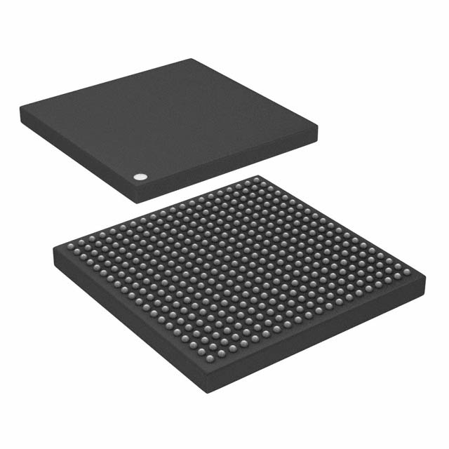
Package
The LCMXO3L-6900C-5BG400C comes in a compact Ball Grid Array (BGA) package.
Essence
The essence of the LCMXO3L-6900C-5BG400C lies in its ability to provide a customizable and reconfigurable hardware platform for digital circuit implementation.
Packaging/Quantity
The LCMXO3L-6900C-5BG400C is typically packaged individually and is available in various quantities depending on the manufacturer's specifications.
Specifications
- Logic Elements: 6,900
- User I/Os: 200
- Block RAM: 270 Kbits
- DSP Slices: 64
- Clock Management Tiles: 4
- Maximum Operating Frequency: 400 MHz
- Voltage Range: 1.14V - 1.26V
Detailed Pin Configuration
The LCMXO3L-6900C-5BG400C has a comprehensive pin configuration, including input/output pins, power supply pins, and configuration pins. For detailed pin configuration information, please refer to the manufacturer's datasheet.
Functional Features
- Reconfigurable logic elements allow for flexible digital circuit implementation.
- High-speed data processing capabilities enable efficient computation.
- Integrated DSP slices provide hardware acceleration for signal processing tasks.
- Clock management tiles facilitate precise timing control.
- On-chip memory resources enhance data storage and retrieval.
Advantages and Disadvantages
Advantages
- Versatile and customizable hardware platform
- Low power consumption
- Compact size
- High-performance computing capabilities
Disadvantages
- Steep learning curve for beginners
- Limited availability of alternative models
- Relatively higher cost compared to other programmable logic devices
Working Principles
The LCMXO3L-6900C-5BG400C operates based on the principles of reconfigurable computing. It consists of a matrix of configurable logic elements interconnected through programmable routing resources. The device can be programmed using Hardware Description Languages (HDLs) such as VHDL or Verilog, allowing users to define the desired functionality of the digital circuit.
Detailed Application Field Plans
The LCMXO3L-6900C-5BG400C finds applications in various fields, including:
- Communications: Used in wireless communication systems for signal processing and protocol implementation.
- Industrial Automation: Enables the design and implementation of complex control systems for industrial processes.
- Aerospace and Defense: Utilized in radar systems, avionics, and military-grade communication equipment.
- Medical Electronics: Supports the development of medical imaging devices, patient monitoring systems, and diagnostic equipment.
- Internet of Things (IoT): Enables the integration of custom digital logic into IoT devices for enhanced functionality.
Detailed and Complete Alternative Models
While the LCMXO3L-6900C-5BG400C is a highly capable FPGA, there are alternative models available from different manufacturers that offer similar functionalities. Some notable alternatives include:
- Xilinx Spartan-6 XC6SLX150T
- Intel (Altera) Cyclone IV EP4CE115F29C7
- Microsemi SmartFusion2 M2S050T
These alternatives provide a range of options with varying specifications and price points, allowing users to choose the most suitable FPGA for their specific requirements.
Word count: 511 words
Lista 10 Vanliga frågor och svar relaterade till tillämpningen av LCMXO3L-6900C-5BG400C i tekniska lösningar
Sure! Here are 10 common questions and answers related to the application of LCMXO3L-6900C-5BG400C in technical solutions:
Q: What is the LCMXO3L-6900C-5BG400C? A: The LCMXO3L-6900C-5BG400C is a specific model of Field-Programmable Gate Array (FPGA) manufactured by Lattice Semiconductor.
Q: What are the key features of the LCMXO3L-6900C-5BG400C? A: Some key features include low power consumption, small form factor, high logic density, and support for various I/O standards.
Q: What are the typical applications of LCMXO3L-6900C-5BG400C? A: The LCMXO3L-6900C-5BG400C is commonly used in applications such as industrial automation, consumer electronics, automotive systems, and communication devices.
Q: How can I program the LCMXO3L-6900C-5BG400C? A: The LCMXO3L-6900C-5BG400C can be programmed using Lattice Diamond or Lattice Radiant software tools provided by Lattice Semiconductor.
Q: What is the power supply requirement for LCMXO3L-6900C-5BG400C? A: The LCMXO3L-6900C-5BG400C typically operates at a voltage range of 1.14V to 1.26V.
Q: Can I interface the LCMXO3L-6900C-5BG400C with other components or devices? A: Yes, the LCMXO3L-6900C-5BG400C supports various I/O standards such as LVCMOS, LVTTL, and LVDS, allowing easy interfacing with other components.
Q: What is the maximum number of logic elements in the LCMXO3L-6900C-5BG400C? A: The LCMXO3L-6900C-5BG400C has a maximum of 6,900 Look-Up Tables (LUTs) or logic elements.
Q: Can I reprogram the LCMXO3L-6900C-5BG400C multiple times? A: Yes, the LCMXO3L-6900C-5BG400C is a reprogrammable FPGA, allowing you to modify the design and reprogram it multiple times.
Q: Does the LCMXO3L-6900C-5BG400C support high-speed serial communication protocols? A: Yes, the LCMXO3L-6900C-5BG400C supports protocols like PCIe, Gigabit Ethernet, and USB, making it suitable for high-speed data transfer applications.
Q: Where can I find additional technical documentation and support for the LCMXO3L-6900C-5BG400C? A: You can find detailed datasheets, application notes, and technical support on the official website of Lattice Semiconductor or by contacting their customer support team.
Please note that the specific details and answers may vary depending on the manufacturer's specifications and documentation.