

LCMXO2-640HC-5SG48C
Product Overview
Category
The LCMXO2-640HC-5SG48C belongs to the category of Field-Programmable Gate Arrays (FPGAs).
Use
This FPGA is commonly used in various electronic applications that require programmable logic devices. It provides designers with flexibility and versatility in implementing digital circuits.
Characteristics
- Low power consumption
- High performance
- Small form factor
- Easy to program and reconfigure
- Wide range of I/O options
Package
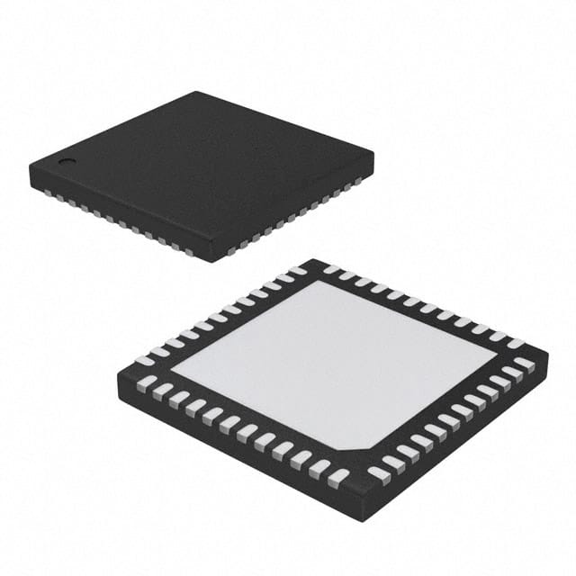
The LCMXO2-640HC-5SG48C comes in a 48-pin small-grid array (SGA) package.
Essence
The essence of this FPGA lies in its ability to be programmed and reprogrammed to perform specific functions, making it suitable for a wide range of applications.
Packaging/Quantity
The LCMXO2-640HC-5SG48C is typically packaged individually and is available in various quantities depending on the manufacturer or distributor.
Specifications
- Logic Cells: 640
- Look-Up Tables (LUTs): 1280
- Flip-Flops: 2560
- Block RAM: 64 Kbits
- Maximum Frequency: 100 MHz
- Operating Voltage: 1.2V
- I/O Voltage: 3.3V
Detailed Pin Configuration
The LCMXO2-640HC-5SG48C has a total of 48 pins. The pin configuration is as follows:
- VCCIO
- GND
- IO_0
- IO_1
- IO_2
- IO_3
- IO_4
- IO_5
- IO_6
- IO_7
- IO_8
- IO_9
- IO_10
- IO_11
- IO_12
- IO_13
- IO_14
- IO_15
- IO_16
- IO_17
- IO_18
- IO_19
- IO_20
- IO_21
- IO_22
- IO_23
- IO_24
- IO_25
- IO_26
- IO_27
- IO_28
- IO_29
- IO_30
- IO_31
- IO_32
- IO_33
- IO_34
- IO_35
- IO_36
- IO_37
- IO_38
- IO_39
- IO_40
- IO_41
- IO_42
- IO_43
- IO_44
- IO_45
Functional Features
- Configurable logic blocks for implementing custom digital circuits
- Programmable interconnects for routing signals between logic blocks
- Dedicated input/output pins for interfacing with external devices
- On-chip memory blocks for storing data
- Clock management resources for synchronizing operations
Advantages and Disadvantages
Advantages
- Flexibility in designing and modifying circuits
- Lower development time compared to custom ASICs
- Cost-effective for low to medium volume production
- Ability to reconfigure the FPGA for different applications
Disadvantages
- Higher power consumption compared to dedicated hardware
- Limited performance compared to specialized processors
- Complexity in programming and debugging
Working Principles
The LCMXO2-640HC-5SG48C operates based on the principles of configurable logic. It consists of a matrix of programmable logic cells and interconnects. The logic cells can be programmed to perform specific functions using a hardware description language (HDL) or a graphical design tool. The interconnects allow signals to be routed between the logic cells, enabling the creation of complex digital circuits.
Detailed Application Field Plans
The LCMXO2-640HC-5SG48C finds applications in various fields, including:
- Embedded systems
- Digital signal processing
- Communication systems
- Industrial automation
- Robotics
- Automotive electronics
- Medical devices
- Aerospace and defense
Detailed and Complete Alternative Models
- LCMXO2-1200HC-4TG144C
- LCMXO2-2000HC-4BG256C
- LCMXO2-4000HC-6TG144C
- LCMXO2-7000HC-5TG144C
- LCMXO2-1200HC-4MG132C
Lista 10 Vanliga frågor och svar relaterade till tillämpningen av LCMXO2-640HC-5SG48C i tekniska lösningar
Sure! Here are 10 common questions and answers related to the application of LCMXO2-640HC-5SG48C in technical solutions:
Q: What is the LCMXO2-640HC-5SG48C? A: The LCMXO2-640HC-5SG48C is a low-cost, low-power FPGA (Field-Programmable Gate Array) device manufactured by Lattice Semiconductor.
Q: What are the key features of LCMXO2-640HC-5SG48C? A: Some key features include 640 Look-Up Tables (LUTs), 64 I/O pins, 4-input look-up tables, on-chip oscillator, and low power consumption.
Q: What are some typical applications of LCMXO2-640HC-5SG48C? A: LCMXO2-640HC-5SG48C can be used in various applications such as industrial control systems, consumer electronics, communication devices, and automotive systems.
Q: How can I program the LCMXO2-640HC-5SG48C? A: The LCMXO2-640HC-5SG48C can be programmed using the Lattice Diamond design software or other compatible programming tools.
Q: What is the power supply requirement for LCMXO2-640HC-5SG48C? A: The LCMXO2-640HC-5SG48C operates at a voltage range of 1.14V to 3.465V, with a recommended operating voltage of 1.2V.
Q: Can I use LCMXO2-640HC-5SG48C for high-speed applications? A: While LCMXO2-640HC-5SG48C is not specifically designed for high-speed applications, it can still be used in moderate-speed designs.
Q: What are the available package options for LCMXO2-640HC-5SG48C? A: LCMXO2-640HC-5SG48C is available in a 48-pin QFN (Quad Flat No-Lead) package.
Q: Can I use LCMXO2-640HC-5SG48C in battery-powered devices? A: Yes, LCMXO2-640HC-5SG48C is known for its low power consumption, making it suitable for battery-powered applications.
Q: Is LCMXO2-640HC-5SG48C suitable for complex designs? A: LCMXO2-640HC-5SG48C is more suitable for small to medium-sized designs due to its limited number of Look-Up Tables (LUTs).
Q: Where can I find technical documentation and support for LCMXO2-640HC-5SG48C? A: You can find technical documentation, datasheets, application notes, and support on the official website of Lattice Semiconductor or by contacting their customer support team.