

LCMXO2-4000HE-6MG184C
Product Overview
Category
The LCMXO2-4000HE-6MG184C belongs to the category of Field Programmable Gate Arrays (FPGAs).
Use
FPGAs are integrated circuits that can be programmed after manufacturing. The LCMXO2-4000HE-6MG184C is specifically designed for use in various electronic systems, including consumer electronics, industrial automation, telecommunications, and automotive applications.
Characteristics
- Low power consumption: The LCMXO2-4000HE-6MG184C is known for its low power consumption, making it suitable for battery-powered devices.
- High performance: This FPGA offers high-speed processing capabilities, enabling efficient execution of complex algorithms.
- Small form factor: With a compact package size, the LCMXO2-4000HE-6MG184C can be easily integrated into space-constrained designs.
- Versatility: It supports a wide range of I/O standards, allowing compatibility with different interfaces.
- Robust packaging: The LCMXO2-4000HE-6MG184C is available in a durable and reliable package, ensuring protection against environmental factors.
Packaging/Quantity
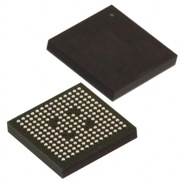
The LCMXO2-4000HE-6MG184C is typically packaged in a surface-mount package, such as a Quad Flat No-Lead (QFN) package. It is commonly sold in reels or trays, with quantities varying based on customer requirements.
Specifications
- FPGA Family: Lattice XO2
- Logic Cells: 4000
- Package Type: QFN
- Package Size: 6mm x 6mm
- I/O Pins: 184
- Operating Voltage: 1.2V
- Maximum Frequency: 100MHz
- Configuration Memory: Flash-based
Detailed Pin Configuration
The LCMXO2-4000HE-6MG184C has a total of 184 I/O pins, which are programmable and can be configured based on the specific application requirements. The pin configuration includes input/output pins, power supply pins, ground pins, and configuration pins.
For a detailed pin configuration diagram, please refer to the datasheet provided by the manufacturer.
Functional Features
- Programmability: The LCMXO2-4000HE-6MG184C offers reconfigurability, allowing users to modify the functionality of the FPGA even after deployment.
- Embedded Memory: It includes embedded memory blocks that can be used for data storage or as lookup tables for implementing complex logic functions.
- Clock Management: The FPGA provides built-in clock management resources, enabling precise control and distribution of clock signals within the system.
- I/O Flexibility: With a large number of I/O pins, the LCMXO2-4000HE-6MG184C supports various communication protocols and interfaces, enhancing its versatility.
Advantages and Disadvantages
Advantages
- Flexibility: The reprogrammable nature of FPGAs allows for quick prototyping and design iterations.
- High Performance: FPGAs offer parallel processing capabilities, making them suitable for computationally intensive tasks.
- Low Power Consumption: The LCMXO2-4000HE-6MG184C's low power consumption makes it ideal for energy-efficient applications.
- Small Form Factor: Its compact size enables integration into space-constrained designs.
Disadvantages
- Complexity: Programming and configuring FPGAs require specialized knowledge and expertise.
- Cost: FPGAs can be more expensive compared to other integrated circuits due to their advanced features and flexibility.
- Limited Resources: The number of logic cells and available memory in an FPGA may impose limitations on the complexity of designs.
Working Principles
FPGAs consist of an array of configurable logic blocks (CLBs) interconnected through programmable routing resources. The LCMXO2-4000HE-6MG184C utilizes look-up tables (LUTs) within the CLBs to implement desired logic functions. These logic functions can be programmed using a Hardware Description Language (HDL) or graphical design tools.
During operation, the FPGA is configured by loading a bitstream into its configuration memory. This bitstream determines the interconnections and functionality of the logic elements within the FPGA. Once configured, the FPGA executes the desired operations based on the programmed logic.
Detailed Application Field Plans
The LCMXO2-4000HE-6MG184C finds applications in various fields, including:
- Consumer Electronics: Used in smart home devices, wearable technology, and multimedia systems.
- Industrial Automation: Employed in control systems, robotics, and factory automation.
- Telecommunications: Utilized in network infrastructure equipment, such as routers and switches.
- Automotive: Integrated into automotive electronics for advanced driver assistance systems (
Lista 10 Vanliga frågor och svar relaterade till tillämpningen av LCMXO2-4000HE-6MG184C i tekniska lösningar
Sure! Here are 10 common questions and answers related to the application of LCMXO2-4000HE-6MG184C in technical solutions:
Q: What is the LCMXO2-4000HE-6MG184C? A: The LCMXO2-4000HE-6MG184C is a low-cost, low-power FPGA (Field-Programmable Gate Array) device manufactured by Lattice Semiconductor.
Q: What are the key features of the LCMXO2-4000HE-6MG184C? A: Some key features include 4000 Look-Up Tables (LUTs), 128 Kbits of embedded Block RAM, 34 I/O pins, and support for various I/O standards.
Q: What are some typical applications of the LCMXO2-4000HE-6MG184C? A: The LCMXO2-4000HE-6MG184C is commonly used in applications such as industrial control systems, consumer electronics, medical devices, and communication equipment.
Q: How can I program the LCMXO2-4000HE-6MG184C? A: The LCMXO2-4000HE-6MG184C can be programmed using Lattice Diamond or Lattice Radiant software tools, which provide a graphical interface for designing and programming the FPGA.
Q: What voltage levels does the LCMXO2-4000HE-6MG184C support? A: The LCMXO2-4000HE-6MG184C supports both 3.3V and 1.2V voltage levels, allowing for compatibility with a wide range of peripherals and interfaces.
Q: Can I use the LCMXO2-4000HE-6MG184C in battery-powered applications? A: Yes, the LCMXO2-4000HE-6MG184C is designed to be power-efficient and can be used in battery-powered applications where low power consumption is critical.
Q: Does the LCMXO2-4000HE-6MG184C support communication protocols like UART or SPI? A: Yes, the LCMXO2-4000HE-6MG184C supports various communication protocols, including UART, SPI, I2C, and GPIO, allowing for easy integration with other devices.
Q: Can I reprogram the LCMXO2-4000HE-6MG184C multiple times? A: Yes, the LCMXO2-4000HE-6MG184C is a reprogrammable FPGA, which means you can modify and reprogram it multiple times as per your application requirements.
Q: Are there any development boards available for the LCMXO2-4000HE-6MG184C? A: Yes, Lattice Semiconductor provides development boards like the LCMXO2-ICE40-HX1K-EVN, which are specifically designed for prototyping and testing with the LCMXO2-4000HE-6MG184C.
Q: Where can I find technical documentation and support for the LCMXO2-4000HE-6MG184C? A: You can find technical documentation, datasheets, application notes, and support resources on the official website of Lattice Semiconductor or by contacting their customer support team.