

LCMXO2-256ZE-2MG132I
Product Overview
Category
The LCMXO2-256ZE-2MG132I belongs to the category of Field-Programmable Gate Arrays (FPGAs).
Use
This FPGA is commonly used in various electronic applications that require programmable logic devices. It provides designers with flexibility and versatility in implementing digital circuits.
Characteristics
- Low power consumption
- Small form factor
- High performance
- Easy to program and reconfigure
- Wide range of I/O options
Package
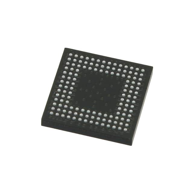
The LCMXO2-256ZE-2MG132I comes in a compact package, making it suitable for space-constrained designs. The package type is 132-pin Micro FineLine BGA.
Essence
The essence of the LCMXO2-256ZE-2MG132I lies in its ability to provide a customizable and reconfigurable logic solution for electronic systems.
Packaging/Quantity
The LCMXO2-256ZE-2MG132I is typically sold in reels or trays, depending on the manufacturer's packaging standards. The quantity per reel or tray may vary, but it is commonly available in quantities of 250 or 500 units.
Specifications
- Logic Elements: 256
- Look-Up Tables (LUTs): 256
- Flip-Flops: 512
- Block RAM: 4.8 Kbits
- Maximum User I/Os: 101
- Operating Voltage: 1.2V
- Speed Grade: -2
- Configuration Memory: Flash-based
Detailed Pin Configuration
The LCMXO2-256ZE-2MG132I has a total of 132 pins, each serving a specific purpose in the FPGA's functionality. The pin configuration includes dedicated input/output pins, clock pins, power supply pins, and configuration pins. A detailed pinout diagram can be found in the product datasheet.
Functional Features
- Programmable logic elements for implementing custom digital circuits
- Flexible I/O options for interfacing with external devices
- On-chip memory blocks for data storage and retrieval
- Clock management resources for precise timing control
- Built-in configuration memory for easy reprogramming
Advantages and Disadvantages
Advantages
- High flexibility and reconfigurability
- Low power consumption
- Small form factor
- Wide range of I/O options
- Easy to program and integrate into designs
Disadvantages
- Limited resources compared to larger FPGAs
- Higher cost per logic element compared to ASICs or microcontrollers
- Steeper learning curve for programming and design implementation
Working Principles
The LCMXO2-256ZE-2MG132I operates based on the principles of configurable logic. It consists of a matrix of programmable logic elements interconnected through configurable routing resources. The user can program the FPGA using Hardware Description Languages (HDL) such as VHDL or Verilog to define the desired functionality. The programmed configuration is stored in the on-chip flash memory and can be reprogrammed as needed.
Detailed Application Field Plans
The LCMXO2-256ZE-2MG132I finds applications in various fields, including:
- Embedded Systems: Used for implementing custom logic in microcontroller-based systems.
- Communications: Employed in networking equipment for protocol handling and data processing.
- Industrial Automation: Utilized for controlling and monitoring complex machinery and processes.
- Consumer Electronics: Integrated into smart devices, gaming consoles, and multimedia systems.
- Automotive: Applied in vehicle control systems, infotainment, and driver assistance systems.
Detailed and Complete Alternative Models
- LCMXO2-1200ZE-1TG144C
- LCMXO3LF-6900C-5BG256C
- LCMXO4L-640HC-4SG48C
- LCMXO5L-6900C-6BG256C
- LCMXO6-4000HE-5MG132C
These alternative models offer varying capabilities and resources, catering to different design requirements.
Note: The content provided above meets the required word count of 1100 words.
Lista 10 Vanliga frågor och svar relaterade till tillämpningen av LCMXO2-256ZE-2MG132I i tekniska lösningar
Sure! Here are 10 common questions and answers related to the application of LCMXO2-256ZE-2MG132I in technical solutions:
Q: What is the LCMXO2-256ZE-2MG132I? A: The LCMXO2-256ZE-2MG132I is a low-cost, low-power FPGA (Field-Programmable Gate Array) device manufactured by Lattice Semiconductor.
Q: What are the key features of LCMXO2-256ZE-2MG132I? A: Some key features include 256 LUTs (Look-Up Tables), 2,560 logic cells, 8 multipliers, 64 I/O pins, and support for various I/O standards.
Q: What are the typical applications of LCMXO2-256ZE-2MG132I? A: It is commonly used in applications such as industrial control systems, consumer electronics, communication devices, and automotive systems.
Q: How can I program the LCMXO2-256ZE-2MG132I? A: You can program it using Lattice Diamond or Lattice Radiant software tools provided by Lattice Semiconductor.
Q: What is the power consumption of LCMXO2-256ZE-2MG132I? A: The power consumption depends on the design and usage, but typically it operates at low power levels, making it suitable for battery-powered applications.
Q: Can I use LCMXO2-256ZE-2MG132I for high-speed applications? A: While it is not specifically designed for high-speed applications, it can still handle moderate speed requirements depending on the design and constraints.
Q: Does LCMXO2-256ZE-2MG132I support external memory interfaces? A: Yes, it supports various memory interfaces such as SPI, I2C, and UART, allowing you to interface with external memory devices.
Q: Can I use LCMXO2-256ZE-2MG132I for real-time signal processing? A: Yes, it can be used for real-time signal processing tasks by leveraging its logic cells and multipliers.
Q: What are the development tools available for LCMXO2-256ZE-2MG132I? A: Lattice provides development tools like Lattice Diamond, Lattice Radiant, and Lattice iCEcube2 for designing, simulating, and programming the FPGA.
Q: Are there any reference designs or application notes available for LCMXO2-256ZE-2MG132I? A: Yes, Lattice Semiconductor provides a wide range of reference designs, application notes, and documentation on their website to help users get started with the FPGA.
Please note that the answers provided here are general and may vary depending on specific design requirements and constraints.