

LCMXO2-1200ZE-2SG32C
Product Overview
Category
The LCMXO2-1200ZE-2SG32C belongs to the category of Field-Programmable Gate Arrays (FPGAs).
Use
FPGAs are integrated circuits that can be programmed and reprogrammed to perform various digital functions. The LCMXO2-1200ZE-2SG32C is specifically designed for applications requiring low power consumption and small form factor.
Characteristics
- Low power consumption
- Small form factor
- High performance
- Flexible and reprogrammable
Package
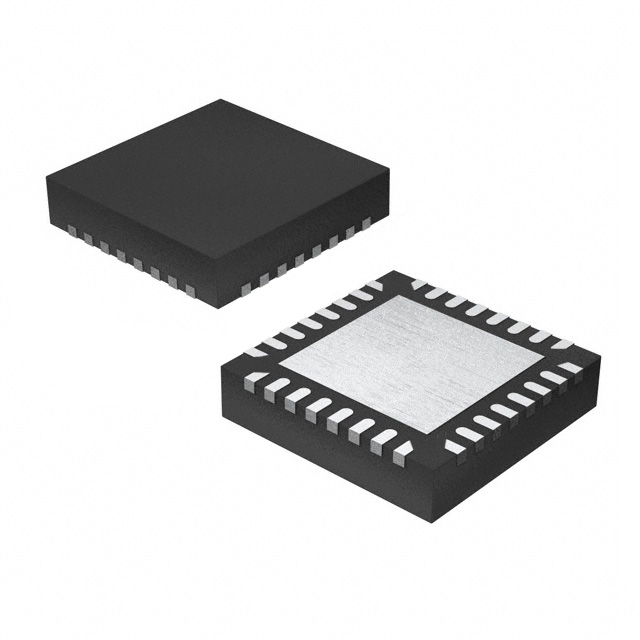
The LCMXO2-1200ZE-2SG32C comes in a 32-pin Small Grid Array (SGA) package.
Essence
The essence of the LCMXO2-1200ZE-2SG32C lies in its ability to provide a customizable digital logic solution with low power consumption and small size.
Packaging/Quantity
The LCMXO2-1200ZE-2SG32C is typically packaged in reels or trays, with quantities varying depending on customer requirements.
Specifications
- Logic Cells: 1200
- Look-Up Tables (LUTs): 1280
- Flip-Flops: 640
- Block RAM: 64 Kbits
- Maximum Frequency: 100 MHz
- I/O Pins: 32
- Voltage Range: 1.2V - 3.3V
- Operating Temperature Range: -40°C to 85°C
Detailed Pin Configuration
The LCMXO2-1200ZE-2SG32C has a total of 32 pins, each serving a specific purpose. The pin configuration is as follows:
- VCCIO
- GND
- IO_0
- IO_1
- IO_2
- IO_3
- IO_4
- IO_5
- IO_6
- IO_7
- IO_8
- IO_9
- IO_10
- IO_11
- IO_12
- IO_13
- IO_14
- IO_15
- IO_16
- IO_17
- IO_18
- IO_19
- IO_20
- IO_21
- IO_22
- IO_23
- IO_24
- IO_25
- IO_26
- IO_27
- IO_28
- IO_29
Functional Features
- Low power consumption allows for energy-efficient operation.
- Small form factor enables integration into space-constrained designs.
- High-performance logic cells and look-up tables provide fast processing capabilities.
- Reprogrammability allows for flexibility in adapting to changing requirements.
Advantages and Disadvantages
Advantages
- Low power consumption makes it suitable for battery-powered devices.
- Small size enables compact and portable designs.
- Reprogrammability allows for iterative development and updates.
- High-performance logic cells ensure efficient processing of digital functions.
Disadvantages
- Limited number of I/O pins may restrict connectivity options.
- Complex programming and configuration process may require specialized knowledge.
- Higher cost compared to fixed-function integrated circuits.
Working Principles
The LCMXO2-1200ZE-2SG32C operates based on the principles of reconfigurable digital logic. It consists of a matrix of programmable logic cells and interconnects that can be configured to implement various digital functions. The device is programmed using a Hardware Description Language (HDL) and the configuration is stored in non-volatile memory. During operation, the programmed logic cells perform the desired digital operations based on the input signals.
Detailed Application Field Plans
The LCMXO2-1200ZE-2SG32C finds applications in various fields, including:
- Internet of Things (IoT) devices
- Wearable technology
- Industrial automation
- Robotics
- Automotive electronics
- Medical devices
- Consumer electronics
In these fields, the FPGA's low power consumption, small form factor, and reprogrammability make it suitable for implementing custom digital functions and adapting to changing requirements.
Detailed and Complete Alternative Models
- LCMXO2-640HC-4SG32C
- LCMXO2-1200HC-4SG32C
- LCMXO2-2000HC-4SG32C
- LCMXO2-4000HC-4SG32C
- LCMXO2-7000HC-4SG32C
Lista 10 Vanliga frågor och svar relaterade till tillämpningen av LCMXO2-1200ZE-2SG32C i tekniska lösningar
Sure! Here are 10 common questions and answers related to the application of LCMXO2-1200ZE-2SG32C in technical solutions:
Q: What is the LCMXO2-1200ZE-2SG32C? A: The LCMXO2-1200ZE-2SG32C is a low-cost, low-power FPGA (Field-Programmable Gate Array) device manufactured by Lattice Semiconductor.
Q: What are the key features of LCMXO2-1200ZE-2SG32C? A: Some key features include 1200 Look-Up Tables (LUTs), 64 Kbits of embedded block RAM, 34 user I/O pins, and support for various I/O standards.
Q: What are some typical applications of LCMXO2-1200ZE-2SG32C? A: It can be used in a wide range of applications such as industrial control systems, consumer electronics, communication devices, and automotive systems.
Q: How can I program the LCMXO2-1200ZE-2SG32C? A: You can program it using Lattice Diamond design software or other compatible development tools provided by Lattice Semiconductor.
Q: What voltage levels does LCMXO2-1200ZE-2SG32C support? A: It supports both 3.3V and 1.2V power supply voltages, making it compatible with a variety of systems.
Q: Can I use LCMXO2-1200ZE-2SG32C for high-speed applications? A: While it is not specifically designed for high-speed applications, it can still handle moderate-speed designs depending on the specific requirements.
Q: Does LCMXO2-1200ZE-2SG32C support external memory interfaces? A: Yes, it supports various memory interfaces such as SPI, I2C, and UART, allowing you to connect external memory devices if needed.
Q: Can I use LCMXO2-1200ZE-2SG32C for real-time signal processing? A: Yes, it can be used for real-time signal processing tasks by implementing appropriate algorithms and logic in the FPGA fabric.
Q: Is LCMXO2-1200ZE-2SG32C suitable for low-power applications? A: Yes, it is designed to be a low-power device, making it suitable for battery-powered or energy-efficient systems.
Q: Are there any development boards available for LCMXO2-1200ZE-2SG32C? A: Yes, Lattice Semiconductor provides development boards like the iCEstick Evaluation Kit that are compatible with LCMXO2-1200ZE-2SG32C for prototyping and development purposes.
Please note that these answers are general and may vary depending on specific design requirements and application scenarios.