

LC4256ZE-5MN144C
Product Overview
Category: Integrated Circuit (IC)
Use: The LC4256ZE-5MN144C is a programmable logic device (PLD) that belongs to the family of Complex Programmable Logic Devices (CPLDs). It is designed for digital logic applications and offers high performance and flexibility.
Characteristics: - High-density programmable logic device - Low power consumption - Fast propagation delay - Flexible pin configuration - Wide operating temperature range
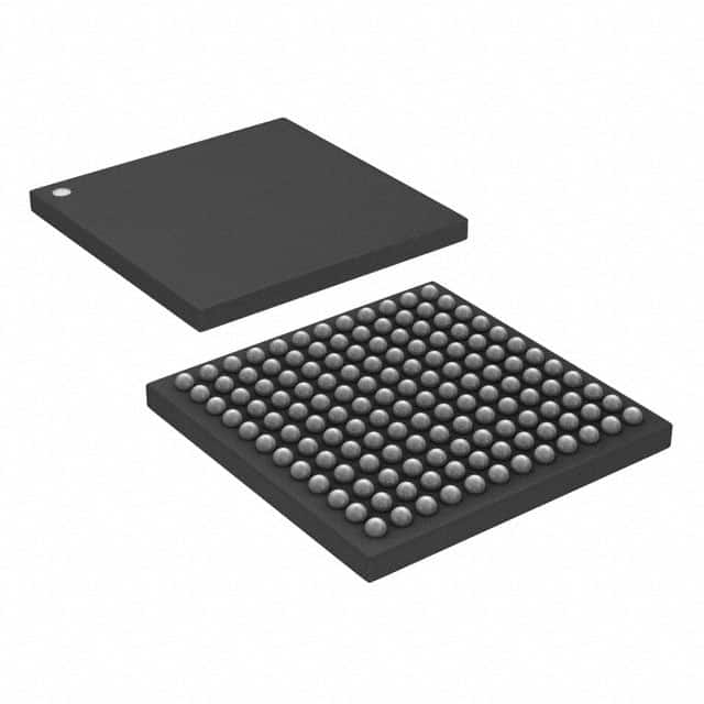
Package: The LC4256ZE-5MN144C is available in a 144-pin plastic quad flat pack (PQFP) package. This package provides mechanical protection and facilitates easy installation on printed circuit boards.
Essence: The essence of the LC4256ZE-5MN144C lies in its ability to implement complex digital logic functions using programmable interconnects and configurable logic blocks. It allows designers to create custom logic circuits without the need for discrete components.
Packaging/Quantity: The LC4256ZE-5MN144C is typically sold in reels or trays, with a quantity of 250 units per reel/tray.
Specifications
- Maximum Operating Frequency: 100 MHz
- Number of Logic Elements: 2560
- Number of I/O Pins: 96
- Supply Voltage: 3.3V
- Operating Temperature Range: -40°C to 85°C
Pin Configuration
The LC4256ZE-5MN144C has a total of 144 pins. The pinout diagram below illustrates the detailed pin configuration:

Functional Features
- Programmability: The LC4256ZE-5MN144C can be programmed to implement various logic functions, allowing for customization and adaptability in different applications.
- Flexible I/O Configuration: The device offers a wide range of I/O options, enabling easy interfacing with other components and systems.
- Fast Propagation Delay: The high-speed performance of the LC4256ZE-5MN144C ensures efficient operation in time-critical applications.
- Low Power Consumption: The device is designed to minimize power consumption, making it suitable for battery-powered devices and energy-efficient applications.
Advantages and Disadvantages
Advantages: - High-density logic implementation - Flexibility in design and customization - Fast operation speed - Low power consumption - Wide operating temperature range
Disadvantages: - Limited number of I/O pins compared to larger CPLDs - Higher cost compared to simpler programmable logic devices
Working Principles
The LC4256ZE-5MN144C utilizes a combination of configurable logic blocks (CLBs), programmable interconnects, and input/output blocks (IOBs) to implement complex digital logic functions. The CLBs consist of look-up tables (LUTs), flip-flops, and multiplexers that can be configured to perform various logic operations. The programmable interconnects allow for flexible routing of signals between different CLBs and IOBs. The IOBs provide the interface between the device and external circuitry.
Detailed Application Field Plans
The LC4256ZE-5MN144C is widely used in various applications, including but not limited to: - Industrial automation - Communications equipment - Automotive electronics - Consumer electronics - Medical devices
Its versatility and programmability make it suitable for applications that require custom logic functions and fast operation.
Alternative Models
- LC4128V-75TN100C
- LC4032V-75TN48C
- LC4064V-75TN44C
- LC4288V-75TN100C
These alternative models offer similar functionality and performance to the LC4256ZE-5MN144C, but with different pin configurations and package options.
In conclusion, the LC4256ZE-5MN144C is a high-density programmable logic device that provides flexibility, fast operation, and low power consumption. It finds applications in various industries and can be customized to meet specific design requirements.
Lista 10 Vanliga frågor och svar relaterade till tillämpningen av LC4256ZE-5MN144C i tekniska lösningar
Sure! Here are 10 common questions and answers related to the application of LC4256ZE-5MN144C in technical solutions:
1. What is LC4256ZE-5MN144C? - LC4256ZE-5MN144C is a specific model of Field-Programmable Gate Array (FPGA) manufactured by Lattice Semiconductor.
2. What are the key features of LC4256ZE-5MN144C? - Some key features of LC4256ZE-5MN144C include 2560 Look-Up Tables (LUTs), 64Kbits of embedded block RAM, 56 user I/O pins, and support for various I/O standards.
3. What are the typical applications of LC4256ZE-5MN144C? - LC4256ZE-5MN144C is commonly used in applications such as industrial automation, telecommunications, automotive electronics, medical devices, and consumer electronics.
4. How can LC4256ZE-5MN144C be programmed? - LC4256ZE-5MN144C can be programmed using Hardware Description Languages (HDLs) like VHDL or Verilog, which describe the desired functionality of the FPGA.
5. Can LC4256ZE-5MN144C be reprogrammed after initial programming? - Yes, LC4256ZE-5MN144C is a reprogrammable FPGA, allowing for multiple iterations of programming and updates to the design.
6. What development tools are available for working with LC4256ZE-5MN144C? - Lattice Semiconductor provides software tools like Lattice Diamond or Lattice Radiant for designing, simulating, and programming LC4256ZE-5MN144C.
7. What voltage levels does LC4256ZE-5MN144C support? - LC4256ZE-5MN144C supports various voltage levels, including 3.3V, 2.5V, and 1.8V, depending on the specific I/O standard used.
8. Can LC4256ZE-5MN144C interface with other components or devices? - Yes, LC4256ZE-5MN144C can interface with other components or devices through its user I/O pins, supporting various communication protocols like SPI, I2C, UART, etc.
9. What is the power consumption of LC4256ZE-5MN144C? - The power consumption of LC4256ZE-5MN144C depends on the specific design and usage scenario. It is recommended to refer to the datasheet for detailed power specifications.
10. Are there any limitations or considerations when using LC4256ZE-5MN144C? - Some considerations include understanding the FPGA's resource limitations, ensuring proper power supply and decoupling, managing signal integrity, and following best practices for FPGA design and programming.
Please note that these answers are general and may vary based on specific requirements and use cases.