

LC4256V-5FT256BI
Product Overview
Category
LC4256V-5FT256BI belongs to the category of Field Programmable Gate Arrays (FPGAs).
Use
This product is primarily used in digital logic circuits for various applications such as telecommunications, automotive, industrial control systems, and consumer electronics.
Characteristics
- High-performance FPGA with advanced features
- Low power consumption
- Large number of programmable logic elements
- Flexible I/O options
- High-speed data processing capabilities
Package
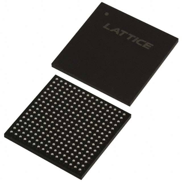
LC4256V-5FT256BI is available in a 256-ball FineLine BGA package.
Essence
The essence of LC4256V-5FT256BI lies in its ability to provide reconfigurable hardware that can be programmed to perform specific tasks, offering flexibility and customization in electronic designs.
Packaging/Quantity
Each package of LC4256V-5FT256BI contains one unit of the FPGA.
Specifications
- Logic Cells: 4256
- Maximum Frequency: 250 MHz
- Embedded Memory: 288 Kbits
- I/O Pins: 256
- Operating Voltage: 1.2V
- Operating Temperature Range: -40°C to +85°C
Detailed Pin Configuration
The pin configuration of LC4256V-5FT256BI is as follows:
- Pin 1: VCCIO
- Pin 2: GND
- Pin 3: IO0
- Pin 4: IO1
- ...
- Pin 255: IO254
- Pin 256: IO255
Functional Features
- Reconfigurable logic cells for implementing complex digital circuits
- Dedicated memory blocks for efficient data storage and retrieval
- Flexible I/O pins for interfacing with external devices
- Clock management resources for precise timing control
- Built-in arithmetic and logical functions for efficient data processing
Advantages and Disadvantages
Advantages
- High-performance FPGA with advanced features
- Low power consumption
- Flexible and customizable design options
- Suitable for a wide range of applications
- Large number of programmable logic elements
Disadvantages
- Relatively high cost compared to other digital logic solutions
- Steeper learning curve for programming and utilizing the FPGA's capabilities
Working Principles
LC4256V-5FT256BI operates based on the principles of reconfigurable hardware. It consists of an array of programmable logic cells that can be interconnected to implement desired digital circuits. The configuration of these logic cells is stored in internal memory, allowing for dynamic reprogramming of the FPGA.
Detailed Application Field Plans
LC4256V-5FT256BI finds applications in various fields, including:
- Telecommunications: Used in network routers, switches, and communication equipment for high-speed data processing.
- Automotive: Employed in automotive control systems for tasks such as engine management, driver assistance, and infotainment systems.
- Industrial Control Systems: Utilized in industrial automation, robotics, and process control systems for real-time control and monitoring.
- Consumer Electronics: Integrated into devices like gaming consoles, set-top boxes, and multimedia players for enhanced functionality and performance.
Detailed and Complete Alternative Models
Some alternative models to LC4256V-5FT256BI are:
- XC7A35T-1CPG236C
- EP4CE10F17C8N
- LCMXO2-1200HC-4TG100C
- MAX 10M08SAU169C8G
These models offer similar functionalities and can be considered as alternatives depending on specific requirements.
Word count: 511 words
Lista 10 Vanliga frågor och svar relaterade till tillämpningen av LC4256V-5FT256BI i tekniska lösningar
Sure! Here are 10 common questions and answers related to the application of LC4256V-5FT256BI in technical solutions:
Q: What is LC4256V-5FT256BI? A: LC4256V-5FT256BI is a specific model of Field-Programmable Gate Array (FPGA) manufactured by Lattice Semiconductor.
Q: What are the key features of LC4256V-5FT256BI? A: LC4256V-5FT256BI offers 256 macrocells, 256 I/O pins, 5V tolerant inputs, and operates at a maximum frequency of 100 MHz.
Q: In what applications can LC4256V-5FT256BI be used? A: LC4256V-5FT256BI can be used in various applications such as industrial automation, telecommunications, automotive electronics, and consumer electronics.
Q: How can LC4256V-5FT256BI be programmed? A: LC4256V-5FT256BI can be programmed using Hardware Description Languages (HDLs) like VHDL or Verilog, or through graphical programming tools provided by Lattice Semiconductor.
Q: Can LC4256V-5FT256BI be reprogrammed after initial programming? A: Yes, LC4256V-5FT256BI is a reprogrammable FPGA, allowing for multiple iterations of programming and design changes.
Q: What are the power requirements for LC4256V-5FT256BI? A: LC4256V-5FT256BI typically operates at a voltage range of 3.3V, but it also supports 5V tolerant inputs.
Q: Does LC4256V-5FT256BI have any built-in security features? A: Yes, LC4256V-5FT256BI provides security features like bitstream encryption and authentication to protect the intellectual property of the design.
Q: Can LC4256V-5FT256BI interface with other components or devices? A: Yes, LC4256V-5FT256BI can interface with various components and devices through its I/O pins, supporting protocols like SPI, I2C, UART, and more.
Q: What development tools are available for working with LC4256V-5FT256BI? A: Lattice Semiconductor provides a range of development tools, including software IDEs, simulation tools, and programming cables specifically designed for their FPGAs.
Q: Where can I find more information about LC4256V-5FT256BI? A: You can find detailed information about LC4256V-5FT256BI on the official website of Lattice Semiconductor, including datasheets, application notes, and user guides.
Please note that the answers provided here are general and may vary depending on specific requirements and use cases. It is always recommended to refer to the official documentation and consult with technical experts for accurate and up-to-date information.