

LC4064C-25T44C
Product Overview
Category: Integrated Circuit (IC)
Use: The LC4064C-25T44C is a programmable logic device (PLD) used for digital circuit design and implementation. It offers versatile functionality and flexibility in various applications.
Characteristics: - High-speed performance - Low power consumption - Compact size - Easy programmability
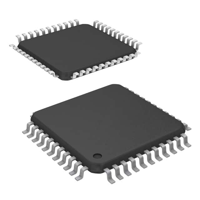
Package: The LC4064C-25T44C comes in a TQFP-44 package, which stands for Thin Quad Flat Package. This package provides a compact form factor and allows for easy integration into electronic systems.
Essence: The essence of the LC4064C-25T44C lies in its ability to provide customizable logic functions, enabling designers to implement complex digital circuits efficiently.
Packaging/Quantity: The LC4064C-25T44C is typically sold in reels or tubes, with each reel/tube containing a specified quantity of ICs. The exact packaging and quantity may vary depending on the supplier.
Specifications
- Operating Voltage: 3.3V
- Speed Grade: 25
- Number of Logic Elements: 64
- Number of I/O Pins: 44
- Programmable Logic Blocks: 32
- Embedded Memory: 1,536 bits
- Clock Management: PLL (Phase-Locked Loop)
- Package Type: TQFP-44
Detailed Pin Configuration
The LC4064C-25T44C has a total of 44 pins, each serving a specific purpose in the circuit design. Here is a detailed pin configuration:
(Pin Number - Pin Name - Description) 1. VCCIO - I/O Power Supply Voltage 2. GND - Ground 3. IO0 - Input/Output Pin 0 4. IO1 - Input/Output Pin 1 5. IO2 - Input/Output Pin 2 6. IO3 - Input/Output Pin 3 7. IO4 - Input/Output Pin 4 8. IO5 - Input/Output Pin 5 9. IO6 - Input/Output Pin 6 10. IO7 - Input/Output Pin 7 11. IO8 - Input/Output Pin 8 12. IO9 - Input/Output Pin 9 13. IO10 - Input/Output Pin 10 14. IO11 - Input/Output Pin 11 15. IO12 - Input/Output Pin 12 16. IO13 - Input/Output Pin 13 17. IO14 - Input/Output Pin 14 18. IO15 - Input/Output Pin 15 19. IO16 - Input/Output Pin 16 20. IO17 - Input/Output Pin 17 21. IO18 - Input/Output Pin 18 22. IO19 - Input/Output Pin 19 23. IO20 - Input/Output Pin 20 24. IO21 - Input/Output Pin 21 25. IO22 - Input/Output Pin 22 26. IO23 - Input/Output Pin 23 27. IO24 - Input/Output Pin 24 28. IO25 - Input/Output Pin 25 29. IO26 - Input/Output Pin 26 30. IO27 - Input/Output Pin 27 31. IO28 - Input/Output Pin 28 32. IO29 - Input/Output Pin 29 33. IO30 - Input/Output Pin 30 34. IO31 - Input/Output Pin 31 35. IO32 - Input/Output Pin 32 36. IO33 - Input/Output Pin 33 37. IO34 - Input/Output Pin 34 38. IO35 - Input/Output Pin 35 39. IO36 - Input/Output Pin 36 40. IO37 - Input/Output Pin 37 41. IO38 - Input/Output Pin 38 42. IO39 - Input/Output Pin 39 43. IO40 - Input/Output Pin 40 44. IO41 - Input/Output Pin 41
Functional Features
The LC4064C-25T44C offers the following functional features:
- Programmability: The device can be programmed to implement various logic functions, allowing for customization and adaptability in different applications.
- High-Speed Performance: With a speed grade of 25, the LC4064C-25T44C operates at high clock frequencies, enabling rapid data processing and response times.
- Low Power Consumption: The IC is designed to minimize power consumption, making it suitable for battery-powered devices or energy-efficient systems.
- **Flexible I
Lista 10 Vanliga frågor och svar relaterade till tillämpningen av LC4064C-25T44C i tekniska lösningar
Sure! Here are 10 common questions and answers related to the application of LC4064C-25T44C in technical solutions:
Question: What is LC4064C-25T44C?
Answer: LC4064C-25T44C is a specific model of a field-programmable gate array (FPGA) manufactured by Lattice Semiconductor.Question: What are the key features of LC4064C-25T44C?
Answer: Some key features of LC4064C-25T44C include 64 macrocells, 64 I/O pins, 25ns maximum propagation delay, and TQFP-44 package.Question: What are the typical applications of LC4064C-25T44C?
Answer: LC4064C-25T44C is commonly used in various technical solutions such as industrial control systems, communication equipment, automotive electronics, and consumer electronics.Question: How can LC4064C-25T44C be programmed?
Answer: LC4064C-25T44C can be programmed using hardware description languages (HDLs) like VHDL or Verilog, or through graphical programming tools provided by Lattice Semiconductor.Question: Can LC4064C-25T44C be reprogrammed after initial programming?
Answer: Yes, LC4064C-25T44C is a reprogrammable FPGA, allowing for multiple programming cycles during its lifespan.Question: What is the power supply requirement for LC4064C-25T44C?
Answer: LC4064C-25T44C requires a power supply voltage of 3.3V.Question: Does LC4064C-25T44C support external memory interfaces?
Answer: Yes, LC4064C-25T44C supports various external memory interfaces such as SDRAM, SRAM, and Flash memory.Question: Can LC4064C-25T44C interface with other digital components or microcontrollers?
Answer: Yes, LC4064C-25T44C can interface with other digital components or microcontrollers through its I/O pins and communication protocols like SPI or I2C.Question: What is the maximum operating frequency of LC4064C-25T44C?
Answer: The maximum operating frequency of LC4064C-25T44C is typically around 100 MHz, but it can vary depending on the design and implementation.Question: Are there any development tools available for designing with LC4064C-25T44C?
Answer: Yes, Lattice Semiconductor provides development tools like Lattice Diamond or iCEcube2 that support designing and programming with LC4064C-25T44C.
Please note that the answers provided here are general and may vary based on specific requirements and application scenarios.