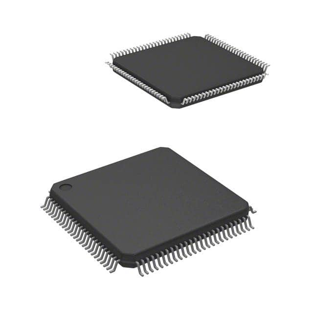
LC4064C-10T100I
Product Overview
Category: Integrated Circuit (IC)
Use: The LC4064C-10T100I is a programmable logic device (PLD) that belongs to the family of Complex Programmable Logic Devices (CPLDs). It is designed for digital logic applications and offers high performance and flexibility.
Characteristics: - High-density programmable logic device - Low power consumption - Fast propagation delay - Wide operating temperature range - Small form factor
Package: The LC4064C-10T100I is available in a TQFP (Thin Quad Flat Package) package. This package provides ease of handling and allows for efficient heat dissipation.
Essence: The essence of the LC4064C-10T100I lies in its ability to implement complex digital logic functions in a single integrated circuit. It offers designers the flexibility to create custom logic circuits tailored to their specific application requirements.
Packaging/Quantity: The LC4064C-10T100I is typically sold in reels or trays, with each reel or tray containing a specified quantity of ICs. The exact packaging and quantity may vary depending on the supplier.
Specifications
- Operating Voltage: 3.3V
- Number of Logic Cells: 64
- Maximum Frequency: 10 MHz
- Number of I/O Pins: 100
- Programmable Logic Blocks: 32
- Embedded Memory: 1,536 bits
- JTAG Boundary Scan Support: Yes
Detailed Pin Configuration
The LC4064C-10T100I has a total of 100 I/O pins, which are used for input and output connections. These pins are arranged in a specific configuration, allowing for easy integration into various circuit designs. For a detailed pin configuration diagram, please refer to the datasheet provided by the manufacturer.
Functional Features
- Programmability: The LC4064C-10T100I can be programmed to implement a wide range of digital logic functions, making it highly versatile for different applications.
- Flexible I/O Configuration: The device offers configurable I/O pins, allowing designers to adapt the interface to match their specific requirements.
- Embedded Memory: The integrated memory blocks enable the storage and retrieval of data within the device itself, reducing the need for external memory components.
- JTAG Boundary Scan Support: The LC4064C-10T100I supports JTAG boundary scan, which facilitates testing and debugging during the development process.
Advantages and Disadvantages
Advantages: - High-density integration - Low power consumption - Fast propagation delay - Flexible programmability - Compact form factor
Disadvantages: - Limited number of logic cells compared to larger CPLDs - Lower maximum frequency compared to some other PLDs
Working Principles
The LC4064C-10T100I operates based on the principles of programmable logic. It consists of an array of logic cells that can be interconnected and programmed to perform desired logic functions. The device is configured using hardware description languages (HDL) or design entry tools, which generate a programming file that defines the desired logic behavior. This programming file is then loaded into the device, enabling it to function according to the specified logic design.
Detailed Application Field Plans
The LC4064C-10T100I finds applications in various fields where digital logic circuits are required. Some potential application areas include: - Industrial automation - Consumer electronics - Communication systems - Automotive electronics - Medical devices
In industrial automation, the LC4064C-10T100I can be used to implement control logic for machinery and equipment. In consumer electronics, it can be utilized for interface control and signal processing. Communication systems can benefit from its ability to handle data routing and protocol conversion. Automotive electronics can leverage its programmability for vehicle control systems. Medical devices can employ the LC4064C-10T100I for signal conditioning and data processing tasks.
Detailed and Complete Alternative Models
- LC4032V-75TN48C: A similar CPLD with 32 logic cells, 75 MHz maximum frequency, and 48 I/O pins.
- LC4128V-75TN144I: Another alternative CPLD with 128 logic cells, 75 MHz maximum frequency, and 144 I/O pins.
- LC4256V-75TN176C: A higher-density CPLD with 256 logic cells, 75 MHz maximum frequency, and 176 I/O pins.
These alternative models offer different combinations of logic capacity, I/O pins, and package options, providing designers with a range of choices based on their specific requirements.
Word count: 615 words
Lista 10 Vanliga frågor och svar relaterade till tillämpningen av LC4064C-10T100I i tekniska lösningar
Sure! Here are 10 common questions and answers related to the application of LC4064C-10T100I in technical solutions:
Q: What is LC4064C-10T100I? A: LC4064C-10T100I is a specific model of a field-programmable gate array (FPGA) manufactured by Lattice Semiconductor.
Q: What are the key features of LC4064C-10T100I? A: Some key features of LC4064C-10T100I include 64 macrocells, 64 I/O pins, 10ns maximum propagation delay, and TQFP-100 package.
Q: In what applications can LC4064C-10T100I be used? A: LC4064C-10T100I can be used in various applications such as industrial control systems, automotive electronics, telecommunications, and consumer electronics.
Q: How can LC4064C-10T100I be programmed? A: LC4064C-10T100I can be programmed using hardware description languages (HDLs) like VHDL or Verilog, or through graphical programming tools provided by Lattice Semiconductor.
Q: What is the power supply requirement for LC4064C-10T100I? A: LC4064C-10T100I requires a single power supply voltage of 3.3V.
Q: Can LC4064C-10T100I interface with other components or devices? A: Yes, LC4064C-10T100I can interface with other components or devices through its I/O pins, which support various standards like LVCMOS, LVTTL, and LVDS.
Q: Is LC4064C-10T100I suitable for high-speed applications? A: Yes, LC4064C-10T100I has a maximum propagation delay of 10ns, making it suitable for many high-speed applications.
Q: Can LC4064C-10T100I be reprogrammed after initial programming? A: Yes, LC4064C-10T100I is a field-programmable device, which means it can be reprogrammed multiple times as per the application requirements.
Q: Are there any development tools available for working with LC4064C-10T100I? A: Yes, Lattice Semiconductor provides development tools like Lattice Diamond and iCEcube2, which facilitate designing, programming, and debugging with LC4064C-10T100I.
Q: Where can I find more information about LC4064C-10T100I? A: You can find more detailed information about LC4064C-10T100I in the datasheet provided by Lattice Semiconductor or on their official website.


