

LC4064B-75T44I
Product Overview
Category: Integrated Circuit (IC)
Use: The LC4064B-75T44I is a programmable logic device (PLD) that belongs to the family of Complex Programmable Logic Devices (CPLDs). It is designed for digital logic applications and offers high-performance, low-power consumption, and flexibility in circuit design.
Characteristics: - High-density integration - Low power consumption - Flexible programming options - Fast propagation delay - Wide operating voltage range
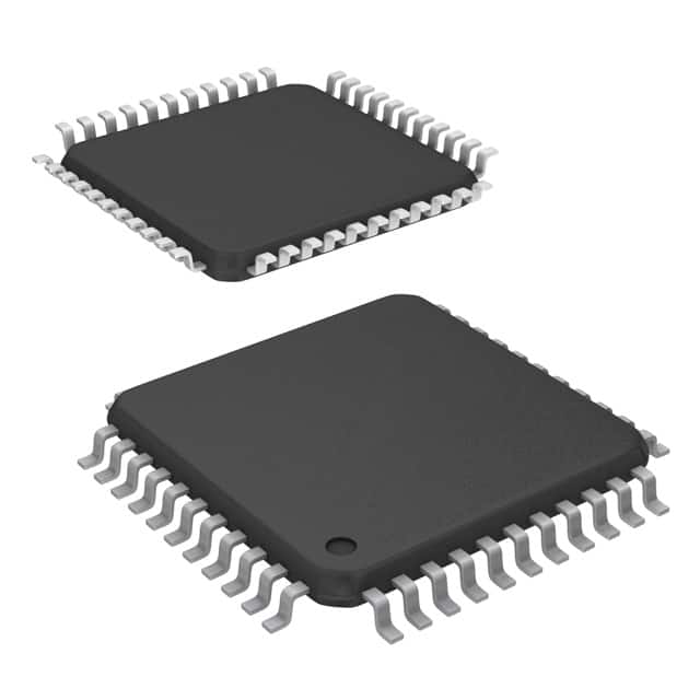
Package: The LC4064B-75T44I is available in a 44-pin Thin Quad Flat Pack (TQFP) package. This package provides a compact form factor and ease of integration into various electronic systems.
Essence: The essence of the LC4064B-75T44I lies in its ability to implement complex digital logic functions using programmable interconnects and configurable logic blocks. It allows designers to create custom logic circuits without the need for discrete components.
Packaging/Quantity: The LC4064B-75T44I is typically sold in reels or tubes, with each reel/tube containing a specified quantity of ICs. The exact packaging and quantity may vary depending on the supplier.
Specifications
- Maximum Operating Frequency: 75 MHz
- Number of Logic Cells: 64
- Number of I/O Pins: 36
- Operating Voltage Range: 3.0V - 3.6V
- Operating Temperature Range: -40°C to +85°C
- Programming Technology: In-system programmable (ISP)
- Package Dimensions: 10mm x 10mm
Detailed Pin Configuration
The LC4064B-75T44I has a total of 44 pins, which are assigned specific functions for input, output, power supply, and programming. The pin configuration is as follows:
(Pin Number) - (Pin Name) - (Function) 1 - VCCIO - I/O Power Supply 2 - GND - Ground 3 - TCK - Test Clock Input 4 - TDI - Test Data Input 5 - TDO - Test Data Output 6 - TMS - Test Mode Select 7 - VCC - Core Power Supply 8-15 - IO[0:7] - General Purpose I/O Pins 16-23 - IO[8:15] - General Purpose I/O Pins 24-31 - IO[16:23] - General Purpose I/O Pins 32-39 - IO[24:31] - General Purpose I/O Pins 40 - GND - Ground 41 - VCCIO - I/O Power Supply 42 - NC - No Connection 43 - NC - No Connection 44 - GND - Ground
Functional Features
The LC4064B-75T44I offers several functional features that make it a versatile choice for digital logic applications:
Programmability: The device can be programmed to implement various logic functions, allowing designers to create custom circuits tailored to their specific requirements.
Flexible Interconnects: The programmable interconnects enable the connection of different logic blocks, facilitating complex circuit designs.
Low Power Consumption: The IC is designed to operate with low power consumption, making it suitable for battery-powered devices or energy-efficient applications.
High-Speed Operation: With a maximum operating frequency of 75 MHz, the LC4064B-75T44I can handle high-speed digital signals effectively.
Wide Operating Voltage Range: The device supports a wide voltage range of 3.0V to 3.6V, providing compatibility with various power supply systems.
Advantages and Disadvantages
Advantages: - High-density integration allows for complex circuit designs in a compact form factor. - Flexible programming options enable customization of logic functions. - Low power consumption makes it suitable for portable and energy-efficient applications. - Fast propagation delay ensures efficient signal processing. - Wide operating voltage range provides compatibility with different power supply systems.
Disadvantages: - Limited number of logic cells may restrict the complexity of certain designs. - Programming and configuring the device may require specialized knowledge and tools. - The 44-pin package may have limitations in terms of I/O count for some applications.
Working Principles
The LC4064B-75T44I operates based on the principles of programmable logic. It consists of configurable logic blocks (CLBs) interconnected through programmable interconnects. The CLBs contain look-up tables (LUTs), flip-flops, and other components that can be configured to implement various logic functions.
During programming, the desired logic functions are defined using a Hardware Description Language (HDL) or a graphical design tool. The configuration data is then loaded into the device, which configures the inter
Lista 10 Vanliga frågor och svar relaterade till tillämpningen av LC4064B-75T44I i tekniska lösningar
Sure! Here are 10 common questions and answers related to the application of LC4064B-75T44I in technical solutions:
Question: What is LC4064B-75T44I?
Answer: LC4064B-75T44I is a specific model of a field-programmable gate array (FPGA) manufactured by Lattice Semiconductor.Question: What are the key features of LC4064B-75T44I?
Answer: Some key features of LC4064B-75T44I include 64 macrocells, 64 input/output pins, 75MHz maximum operating frequency, and a TQFP-44 package.Question: In what applications can LC4064B-75T44I be used?
Answer: LC4064B-75T44I can be used in various applications such as industrial automation, telecommunications, automotive electronics, and consumer electronics.Question: How can LC4064B-75T44I be programmed?
Answer: LC4064B-75T44I can be programmed using hardware description languages (HDL) like VHDL or Verilog, which are then synthesized into a bitstream file that can be loaded onto the FPGA.Question: Can LC4064B-75T44I be reprogrammed after initial programming?
Answer: Yes, LC4064B-75T44I is a field-programmable device, meaning it can be reprogrammed multiple times to implement different designs or functionalities.Question: What tools are available for programming LC4064B-75T44I?
Answer: Lattice Semiconductor provides software tools like Lattice Diamond or iCEcube2 for designing, synthesizing, and programming LC4064B-75T44I.Question: What is the power supply requirement for LC4064B-75T44I?
Answer: LC4064B-75T44I typically operates with a 3.3V power supply, but it also supports a wide voltage range from 2.25V to 3.6V.Question: Can LC4064B-75T44I interface with other components or devices?
Answer: Yes, LC4064B-75T44I can interface with various components and devices through its input/output pins, allowing communication and integration within a larger system.Question: Are there any limitations or considerations when using LC4064B-75T44I?
Answer: Some considerations include the limited number of macrocells and I/O pins, as well as the maximum operating frequency. These factors should be taken into account during design and implementation.Question: Where can I find more information about LC4064B-75T44I?
Answer: You can find more detailed information about LC4064B-75T44I in the datasheet provided by Lattice Semiconductor or by visiting their official website.