

ICE40UL1K-SWG16ITR50
Product Overview
- Category: Integrated Circuit (IC)
- Use: Programmable Logic Device (PLD)
- Characteristics: Low-power, small form factor, high-performance
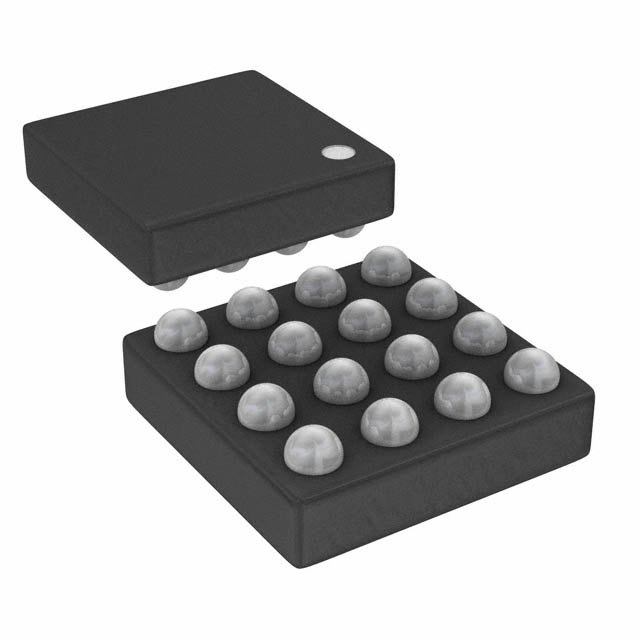
- Package: SWG16ITR50
- Essence: The ICE40UL1K-SWG16ITR50 is a programmable logic device designed for low-power applications. It offers high performance in a small form factor package.
- Packaging/Quantity: The ICE40UL1K-SWG16ITR50 is available in the SWG16ITR50 package and is typically sold in quantities of one.
Specifications
- Logic Elements: 1280
- RAM Bits: 64,000
- User I/O Pins: 48
- Operating Voltage: 1.2V
- Operating Temperature Range: -40°C to 85°C
- Speed Grade: Standard
Detailed Pin Configuration
The ICE40UL1K-SWG16ITR50 has a total of 48 user I/O pins. These pins can be configured as inputs or outputs based on the application requirements. The pin configuration is as follows:
- Pin 1: VCCIO
- Pin 2: GND
- Pin 3: IO0
- Pin 4: IO1
- ...
- Pin 48: IO47
Functional Features
- Low-power consumption: The ICE40UL1K-SWG16ITR50 is designed to operate at low power, making it suitable for battery-powered devices and energy-efficient applications.
- Small form factor: The compact size of the device allows for easy integration into space-constrained designs.
- High-performance: Despite its small size, the ICE40UL1K-SWG16ITR50 offers high-performance capabilities, making it suitable for demanding applications.
Advantages and Disadvantages
Advantages
- Low-power consumption
- Small form factor
- High-performance capabilities
- Easy integration into space-constrained designs
Disadvantages
- Limited logic elements compared to higher-end programmable logic devices
- Limited RAM capacity compared to higher-end programmable logic devices
Working Principles
The ICE40UL1K-SWG16ITR50 is based on the field-programmable gate array (FPGA) technology. It consists of a matrix of configurable logic blocks (CLBs) that can be programmed to perform various logic functions. The device is programmed using a hardware description language (HDL) such as Verilog or VHDL. Once programmed, the device can execute the desired logic operations.
Detailed Application Field Plans
The ICE40UL1K-SWG16ITR50 is suitable for a wide range of applications, including:
- Internet of Things (IoT) devices: The low-power consumption and small form factor make it ideal for IoT devices that require long battery life and compact size.
- Wearable devices: The small size and high-performance capabilities make it suitable for wearable devices such as smartwatches and fitness trackers.
- Industrial automation: The device's high-performance capabilities make it suitable for industrial automation applications that require real-time processing and control.
- Consumer electronics: The ICE40UL1K-SWG16ITR50 can be used in various consumer electronics products, including smartphones, tablets, and gaming consoles.
Detailed and Complete Alternative Models
- ICE40LP1K-CM36ITR50: Similar to the ICE40UL1K-SWG16ITR50, but with a different package and pin configuration.
- ICE40HX1K-VQ100C: A higher-end alternative with more logic elements and RAM capacity.
- ICE40UP5K-SG48I: A larger alternative with increased logic elements and I/O pins.
These alternative models offer different features and capabilities, allowing designers to choose the most suitable option for their specific application requirements.
Word count: 511 words
Lista 10 Vanliga frågor och svar relaterade till tillämpningen av ICE40UL1K-SWG16ITR50 i tekniska lösningar
Sure! Here are 10 common questions and answers related to the application of ICE40UL1K-SWG16ITR50 in technical solutions:
Q1: What is the ICE40UL1K-SWG16ITR50? A1: The ICE40UL1K-SWG16ITR50 is a low-power, small form factor FPGA (Field-Programmable Gate Array) device manufactured by Lattice Semiconductor.
Q2: What are the key features of the ICE40UL1K-SWG16ITR50? A2: Some key features include 1280 Look-Up Tables (LUTs), 64 Kbits of embedded block RAM, 8 global clocks, and support for up to 16 input/output pins.
Q3: What are some typical applications of the ICE40UL1K-SWG16ITR50? A3: The ICE40UL1K-SWG16ITR50 is commonly used in applications such as IoT devices, sensor interfaces, motor control, portable medical devices, and more.
Q4: How can I program the ICE40UL1K-SWG16ITR50? A4: The ICE40UL1K-SWG16ITR50 can be programmed using the Lattice Diamond design software or the open-source Project IceStorm toolchain.
Q5: What is the power consumption of the ICE40UL1K-SWG16ITR50? A5: The ICE40UL1K-SWG16ITR50 is designed for low-power applications and has a typical power consumption of around 25-50 mW.
Q6: Can I use the ICE40UL1K-SWG16ITR50 in battery-powered devices? A6: Yes, the low-power characteristics of the ICE40UL1K-SWG16ITR50 make it suitable for battery-powered devices where power efficiency is crucial.
Q7: How many I/O pins does the ICE40UL1K-SWG16ITR50 support? A7: The ICE40UL1K-SWG16ITR50 supports up to 16 input/output pins, which can be configured as either single-ended or differential I/Os.
Q8: Can I interface the ICE40UL1K-SWG16ITR50 with other components or microcontrollers? A8: Yes, the ICE40UL1K-SWG16ITR50 can be easily interfaced with other components or microcontrollers using standard communication protocols such as SPI or I2C.
Q9: What is the maximum clock frequency supported by the ICE40UL1K-SWG16ITR50? A9: The ICE40UL1K-SWG16ITR50 supports a maximum clock frequency of up to 133 MHz.
Q10: Are there any development boards available for prototyping with the ICE40UL1K-SWG16ITR50? A10: Yes, Lattice Semiconductor offers development boards like the iCEstick and the iCE40 UltraPlus Breakout Board that are compatible with the ICE40UL1K-SWG16ITR50 for prototyping and evaluation purposes.
Please note that these answers are general and may vary depending on specific requirements and use cases.