

ICE40LP1K-CM49TR
Product Overview
- Category: Integrated Circuit
- Use: Programmable Logic Device (PLD)
- Characteristics: Low power consumption, small form factor, high performance
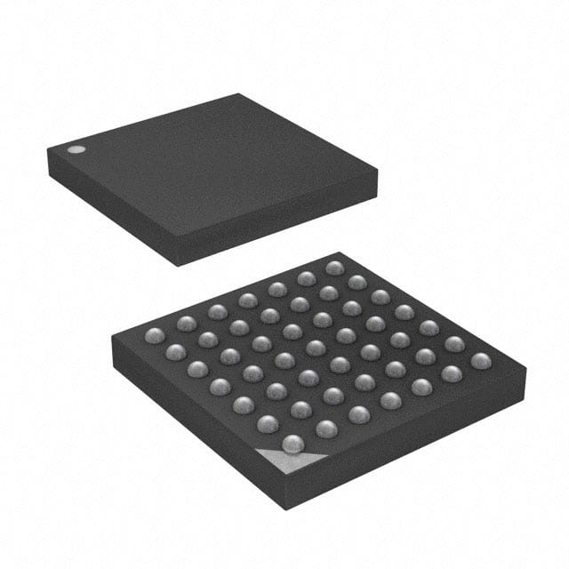
- Package: CM49TR
- Essence: The ICE40LP1K-CM49TR is a programmable logic device designed for low power applications. It offers high performance and flexibility in a compact package.
- Packaging/Quantity: Available in tape and reel packaging with a quantity of 2500 units per reel.
Specifications
- Logic Cells: 1280
- User I/O Pins: 49
- Operating Voltage: 1.2V
- Operating Temperature Range: -40°C to 85°C
- Speed Grade: Standard (4)
Detailed Pin Configuration
The ICE40LP1K-CM49TR has a total of 49 user I/O pins. The pin configuration is as follows:
- Pin 1: VCCIO
- Pin 2: GND
- Pin 3: IO0
- Pin 4: IO1
- ...
- Pin 49: IO48
Functional Features
- Low power consumption: The ICE40LP1K-CM49TR is designed to operate at low power levels, making it suitable for battery-powered devices and energy-efficient applications.
- High performance: Despite its low power consumption, the device offers high performance and can handle complex logic functions.
- Small form factor: The compact package allows for easy integration into space-constrained designs.
- Flexibility: The device is programmable, allowing users to configure it for various applications.
Advantages and Disadvantages
Advantages: - Low power consumption enables energy-efficient designs. - High performance for handling complex logic functions. - Compact form factor allows for easy integration. - Programmability provides flexibility for different applications.
Disadvantages: - Limited number of user I/O pins may restrict the complexity of designs. - Standard speed grade may not meet the requirements of high-speed applications.
Working Principles
The ICE40LP1K-CM49TR is based on a programmable logic architecture. It consists of configurable logic blocks (CLBs), interconnect resources, and input/output blocks (IOBs). The CLBs can be programmed to implement various logic functions, while the interconnect resources allow for the routing of signals between different CLBs. The IOBs provide the interface between the device and external components.
When programmed, the device operates by receiving inputs, processing them through the configured logic functions, and producing outputs accordingly. The low power consumption is achieved through efficient circuit design and power management techniques.
Detailed Application Field Plans
The ICE40LP1K-CM49TR is suitable for a wide range of applications, including:
- Internet of Things (IoT) devices: The low power consumption and small form factor make it ideal for IoT devices that require long battery life and compact size.
- Consumer electronics: The device can be used in portable devices, such as smartphones and tablets, where power efficiency and performance are crucial.
- Industrial automation: Its high performance and flexibility make it suitable for industrial control systems and automation equipment.
- Automotive electronics: The device can be utilized in automotive applications, such as advanced driver-assistance systems (ADAS) and infotainment systems.
Detailed and Complete Alternative Models
- ICE40LP384-CM81: A smaller variant with 384 logic cells and 81 user I/O pins.
- ICE40LP8K-CM225: A higher-end model with 8000 logic cells and 225 user I/O pins.
- ICE40UP5K-SG48: An ultra-low power variant with 5280 logic cells and 48 user I/O pins.
These alternative models offer different levels of performance, I/O capabilities, and power consumption to cater to diverse application requirements.
Word count: 510 words
Lista 10 Vanliga frågor och svar relaterade till tillämpningen av ICE40LP1K-CM49TR i tekniska lösningar
Sure! Here are 10 common questions and answers related to the application of ICE40LP1K-CM49TR in technical solutions:
Q1: What is ICE40LP1K-CM49TR? A1: ICE40LP1K-CM49TR is a low-power, small form factor FPGA (Field-Programmable Gate Array) device manufactured by Lattice Semiconductor.
Q2: What are the key features of ICE40LP1K-CM49TR? A2: Some key features of ICE40LP1K-CM49TR include low power consumption, small package size, high performance, and reprogrammability.
Q3: What are the typical applications of ICE40LP1K-CM49TR? A3: ICE40LP1K-CM49TR is commonly used in applications such as IoT devices, sensor interfaces, motor control, audio/video processing, and low-power embedded systems.
Q4: How does ICE40LP1K-CM49TR achieve low power consumption? A4: ICE40LP1K-CM49TR utilizes a combination of low-power design techniques, such as clock gating, power optimization algorithms, and dynamic power management, to minimize power consumption.
Q5: Can ICE40LP1K-CM49TR be programmed by the user? A5: Yes, ICE40LP1K-CM49TR is a programmable device. Users can program it using hardware description languages (HDLs) like Verilog or VHDL.
Q6: What tools are available for programming ICE40LP1K-CM49TR? A6: Lattice Semiconductor provides the Lattice Diamond software suite, which includes a graphical design tool and a compiler for programming ICE40LP1K-CM49TR.
Q7: What is the maximum number of logic elements (LEs) in ICE40LP1K-CM49TR? A7: ICE40LP1K-CM49TR has a maximum of 1280 logic elements (LEs), which can be used to implement various digital circuits.
Q8: Can ICE40LP1K-CM49TR interface with other components or devices? A8: Yes, ICE40LP1K-CM49TR supports various I/O standards and can interface with other components or devices such as sensors, displays, memory, and communication interfaces.
Q9: Is ICE40LP1K-CM49TR suitable for high-speed applications? A9: While ICE40LP1K-CM49TR is not specifically designed for high-speed applications, it can still handle moderate-speed designs effectively.
Q10: Are there any development boards available for ICE40LP1K-CM49TR? A10: Yes, Lattice Semiconductor offers development boards like the iCEstick and the iCE40 UltraPlus Breakout Board, which are compatible with ICE40LP1K-CM49TR and provide an easy way to prototype and test designs.
Please note that these answers are general and may vary depending on specific requirements and use cases.