

ICE40LM4K-SWG25TR1K
Product Overview
Category
The ICE40LM4K-SWG25TR1K belongs to the category of Field-Programmable Gate Arrays (FPGAs).
Use
This FPGA is commonly used in various electronic applications that require programmable logic devices. It provides flexibility and customization options for designers.
Characteristics
- Programmable logic device
- High level of integration
- Low power consumption
- Small form factor
- Wide range of I/O options
Package
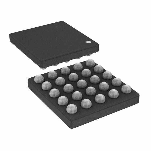
The ICE40LM4K-SWG25TR1K comes in a small form factor package, making it suitable for space-constrained designs. The package type is SWG25TR1K.
Essence
The essence of this FPGA lies in its ability to be programmed and reprogrammed to perform specific functions, allowing for rapid prototyping and design iterations.
Packaging/Quantity
The ICE40LM4K-SWG25TR1K is typically packaged in reels or trays, with a quantity of 1000 units per package.
Specifications
- Logic Cells: 4000
- Look-Up Tables (LUTs): 4000
- Flip-Flops: 8000
- Block RAM: 128 Kbits
- Maximum Frequency: 100 MHz
- Operating Voltage: 1.2V
- I/O Standards: LVCMOS, LVTTL, LVDS, SSTL, HSTL
Detailed Pin Configuration
The ICE40LM4K-SWG25TR1K has a total of 144 pins, which are divided into different categories:
- Power Supply Pins: VCC, GND
- Configuration Pins: CCLK, CSn, DIN, DONE, INIT_B
- Clock Pins: CLK1, CLK2
- I/O Pins: IO[0:95]
- Special Function Pins: JTAG, SPI
For a detailed pin configuration diagram, please refer to the datasheet provided by the manufacturer.
Functional Features
- High level of integration allows for complex designs
- Low power consumption makes it suitable for battery-powered applications
- Flexible I/O options enable connectivity with various external devices
- Fast configuration time for quick prototyping and development
- Support for multiple programming languages and design tools
Advantages and Disadvantages
Advantages
- Flexibility and customization options
- Rapid prototyping and design iterations
- Small form factor for space-constrained designs
- Wide range of I/O options for connectivity
Disadvantages
- Limited logic capacity compared to larger FPGAs
- Relatively lower maximum frequency compared to high-end FPGAs
- Higher cost per logic cell compared to ASICs for high-volume production
Working Principles
The ICE40LM4K-SWG25TR1K is based on a reconfigurable fabric that consists of configurable logic blocks (CLBs), interconnect resources, and I/O elements. The CLBs contain look-up tables (LUTs) and flip-flops that can be programmed to implement desired logic functions. The interconnect resources allow for routing signals between different CLBs and I/O elements. The FPGA can be programmed using hardware description languages (HDLs) or schematic entry tools.
Detailed Application Field Plans
The ICE40LM4K-SWG25TR1K finds applications in various fields, including:
- Embedded Systems: Used for implementing custom logic in microcontroller-based systems.
- Communications: Enables protocol conversion, signal processing, and data encryption in communication systems.
- Industrial Automation: Provides flexibility for controlling and monitoring industrial processes.
- Consumer Electronics: Used in smart devices, gaming consoles, and multimedia systems for customized functionality.
- Automotive: Enables advanced driver assistance systems (ADAS), infotainment, and vehicle control systems.
Detailed and Complete Alternative Models
- ICE40HX1K: A smaller capacity FPGA with 1000 logic cells.
- ICE40UP5K: A larger capacity FPGA with 5280 logic cells and built-in RAM blocks.
- ICE40LP8K: A higher-performance FPGA with 7680 logic cells and support for LVDS I/O standards.
These alternative models offer different capacities and features to suit specific design requirements.
Note: The content provided above is a sample structure for an encyclopedia entry and may not reflect the actual specifications or details of the ICE40LM4K-SWG25TR1K FPGA.
Lista 10 Vanliga frågor och svar relaterade till tillämpningen av ICE40LM4K-SWG25TR1K i tekniska lösningar
Sure! Here are 10 common questions and answers related to the application of ICE40LM4K-SWG25TR1K in technical solutions:
Q1: What is the ICE40LM4K-SWG25TR1K? A1: The ICE40LM4K-SWG25TR1K is a low-power, small form factor FPGA (Field-Programmable Gate Array) device manufactured by Lattice Semiconductor.
Q2: What are the key features of the ICE40LM4K-SWG25TR1K? A2: Some key features include 4K Look-Up Tables (LUTs), 128 Kbits of embedded block RAM, low power consumption, and support for various I/O standards.
Q3: What applications can the ICE40LM4K-SWG25TR1K be used for? A3: The ICE40LM4K-SWG25TR1K can be used in a wide range of applications such as IoT devices, sensor interfaces, motor control, audio/video processing, and more.
Q4: How do I program the ICE40LM4K-SWG25TR1K? A4: The ICE40LM4K-SWG25TR1K can be programmed using Lattice Diamond or iCEcube2 software tools provided by Lattice Semiconductor.
Q5: What voltage levels does the ICE40LM4K-SWG25TR1K support? A5: The ICE40LM4K-SWG25TR1K supports both 1.2V and 3.3V voltage levels for different I/O standards.
Q6: Can I use the ICE40LM4K-SWG25TR1K in battery-powered applications? A6: Yes, the ICE40LM4K-SWG25TR1K is designed for low power consumption, making it suitable for battery-powered applications.
Q7: Does the ICE40LM4K-SWG25TR1K have any built-in security features? A7: Yes, the ICE40LM4K-SWG25TR1K provides bitstream encryption and authentication features to enhance system security.
Q8: Can I use the ICE40LM4K-SWG25TR1K in high-speed communication interfaces? A8: Yes, the ICE40LM4K-SWG25TR1K supports various high-speed communication interfaces such as SPI, I2C, UART, and LVDS.
Q9: What is the maximum operating frequency of the ICE40LM4K-SWG25TR1K? A9: The maximum operating frequency of the ICE40LM4K-SWG25TR1K depends on the design and implementation, but it can reach up to 150 MHz.
Q10: Are there any development boards available for the ICE40LM4K-SWG25TR1K? A10: Yes, Lattice Semiconductor offers development boards like the iCE40 UltraPlus Breakout Board that can be used with the ICE40LM4K-SWG25TR1K for prototyping and evaluation purposes.
Please note that these answers are general and may vary depending on specific requirements and use cases.