

IS25WP128F-JKLE
Product Overview
Category
IS25WP128F-JKLE belongs to the category of flash memory devices.
Use
It is primarily used for data storage and retrieval in electronic devices.
Characteristics
- Non-volatile memory
- High-speed read and write operations
- Compact size
- Low power consumption
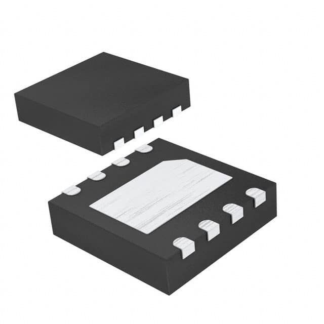
Package
IS25WP128F-JKLE is available in a small form factor package, suitable for integration into various electronic devices.
Essence
The essence of IS25WP128F-JKLE lies in its ability to store and retrieve digital information reliably and efficiently.
Packaging/Quantity
The product is typically packaged individually and is available in varying quantities depending on the manufacturer's specifications.
Specifications
- Memory Type: Flash
- Capacity: 128 Megabits (16 Megabytes)
- Interface: Serial Peripheral Interface (SPI)
- Operating Voltage: 2.7V - 3.6V
- Operating Temperature Range: -40°C to +85°C
- Data Retention: Up to 20 years
- Erase/Program Cycles: Up to 100,000 cycles
Detailed Pin Configuration
The IS25WP128F-JKLE has the following pin configuration:
- VCC - Power supply voltage
- GND - Ground
- HOLD - Suspends ongoing data transfer
- WP - Write Protect
- SCK - Serial Clock
- SI - Serial Input
- SO - Serial Output
- CS - Chip Select
Functional Features
- High-speed data transfer
- Flexible erase and programming options
- Sector protection mechanism
- Software and hardware write protection
- Efficient power management
Advantages
- Compact size allows for easy integration into various devices
- High-speed read and write operations enhance overall performance
- Low power consumption prolongs battery life
- Sector protection mechanism ensures data integrity and security
Disadvantages
- Limited storage capacity compared to other flash memory devices
- Relatively higher cost per unit of storage compared to traditional hard drives
Working Principles
IS25WP128F-JKLE utilizes the principles of flash memory technology. It stores digital information by trapping electric charges within floating gate transistors. These charges represent binary data, which can be read or modified through specific electrical signals.
Detailed Application Field Plans
IS25WP128F-JKLE finds applications in various electronic devices, including but not limited to:
- Smartphones and tablets
- Digital cameras
- Portable media players
- Automotive electronics
- Industrial control systems
Detailed and Complete Alternative Models
- IS25LP128F-JKLE
- MX25L12845E
- W25Q128JVSIQ
- S25FL128SAGMFI011
These alternative models offer similar functionality and specifications to IS25WP128F-JKLE, providing options for different design requirements.
Word count: 365 words
Lista 10 Vanliga frågor och svar relaterade till tillämpningen av IS25WP128F-JKLE i tekniska lösningar
Sure! Here are 10 common questions and answers related to the application of IS25WP128F-JKLE in technical solutions:
Q: What is IS25WP128F-JKLE? A: IS25WP128F-JKLE is a specific model of Serial NOR Flash memory chip manufactured by a company called ISSI. It has a capacity of 128 megabits (16 megabytes) and is commonly used in various electronic devices.
Q: What are the main features of IS25WP128F-JKLE? A: The main features of IS25WP128F-JKLE include high-speed read and write operations, low power consumption, wide operating voltage range, and compatibility with standard SPI (Serial Peripheral Interface) communication protocol.
Q: In which applications can IS25WP128F-JKLE be used? A: IS25WP128F-JKLE is commonly used in applications such as automotive electronics, industrial control systems, consumer electronics, medical devices, and Internet of Things (IoT) devices.
Q: How can IS25WP128F-JKLE be interfaced with a microcontroller or processor? A: IS25WP128F-JKLE uses the SPI interface for communication. It requires four signal lines: Serial Clock (SCK), Chip Select (CS), Master Out Slave In (MOSI), and Master In Slave Out (MISO).
Q: What is the maximum data transfer speed supported by IS25WP128F-JKLE? A: IS25WP128F-JKLE supports a maximum clock frequency of up to 104 MHz, allowing for fast data transfer between the memory chip and the microcontroller/processor.
Q: Can IS25WP128F-JKLE be easily soldered onto a PCB? A: Yes, IS25WP128F-JKLE comes in a standard surface-mount package (such as SOP or WSON), which can be easily soldered onto a printed circuit board (PCB) using conventional soldering techniques.
Q: Does IS25WP128F-JKLE support hardware and software write protection? A: Yes, IS25WP128F-JKLE provides both hardware and software write protection features to prevent accidental or unauthorized modification of the stored data.
Q: What is the typical operating voltage range for IS25WP128F-JKLE? A: The typical operating voltage range for IS25WP128F-JKLE is from 2.7V to 3.6V, making it compatible with a wide range of power supply voltages commonly used in electronic systems.
Q: Can IS25WP128F-JKLE withstand harsh environmental conditions? A: Yes, IS25WP128F-JKLE is designed to operate reliably in a wide temperature range (-40°C to +85°C) and can withstand mechanical shocks and vibrations typically encountered in industrial and automotive applications.
Q: Are there any specific programming requirements for IS25WP128F-JKLE? A: IS25WP128F-JKLE requires specific commands and protocols to perform read, write, erase, and other operations. These instructions are provided in the datasheet and can be implemented using standard SPI communication libraries or drivers.
Please note that the answers provided here are general and may vary depending on the specific implementation and requirements of your technical solution. It is always recommended to refer to the official datasheet and documentation provided by the manufacturer for accurate and detailed information.