

EPM570F100A5N
Product Overview
Category
EPM570F100A5N belongs to the category of Field Programmable Gate Arrays (FPGAs).
Use
This FPGA is designed for various applications that require high-performance digital logic circuits. It provides a flexible and reconfigurable platform for implementing complex digital designs.
Characteristics
- High-performance FPGA with advanced features
- Reconfigurable architecture allows for flexibility in design implementation
- Offers a wide range of logic elements, memory blocks, and I/O interfaces
- Supports high-speed data processing and efficient power consumption
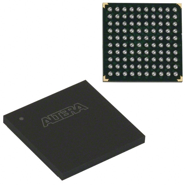
Package
EPM570F100A5N comes in a compact package suitable for surface mount technology (SMT) assembly. The package ensures easy integration into electronic systems and provides protection against environmental factors.
Essence
The essence of EPM570F100A5N lies in its ability to provide a customizable and versatile solution for digital circuit design. Its reprogrammable nature allows for quick iterations and modifications during the development process.
Packaging/Quantity
EPM570F100A5N is typically packaged in reels or trays, depending on the manufacturer's specifications. The quantity per package may vary, but it is commonly available in quantities suitable for both prototyping and production purposes.
Specifications
- Logic Elements: 57,000
- Memory Blocks: 4,608
- Maximum User I/Os: 350
- Maximum Operating Frequency: 300 MHz
- Embedded Multipliers: 288
- On-Chip RAM: 1,152 Kbits
- Configuration Bits: 100,000
Detailed Pin Configuration
The pin configuration of EPM570F100A5N is as follows:
| Pin Number | Pin Name | Description | |------------|----------|-------------| | 1 | VCCINT | Power supply voltage for internal circuitry | | 2 | GND | Ground reference | | 3 | VCCIO | Power supply voltage for I/O banks | | 4 | IO1 | General-purpose I/O pin 1 | | ... | ... | ... | | 350 | IO350 | General-purpose I/O pin 350 |
Note: This is a simplified representation of the pin configuration. The actual device may have additional pins and specialized functions.
Functional Features
- High-speed data processing capabilities
- Configurable logic elements for implementing complex digital designs
- On-chip memory blocks for efficient data storage
- Embedded multipliers for performing arithmetic operations
- Flexible I/O interfaces for seamless integration with external devices
Advantages and Disadvantages
Advantages
- Flexibility in design implementation due to reconfigurable nature
- High-performance capabilities enable complex applications
- Efficient power consumption for improved energy efficiency
- Wide range of I/O interfaces for versatile connectivity options
Disadvantages
- Steep learning curve for beginners due to complexity
- Higher cost compared to traditional fixed-function integrated circuits
- Limited availability of alternative models with similar specifications
Working Principles
EPM570F100A5N operates based on the principles of field-programmable gate arrays. It consists of configurable logic elements, memory blocks, and I/O interfaces interconnected through programmable routing resources. The device can be programmed using hardware description languages (HDL) or graphical tools to define the desired functionality. Once programmed, the FPGA executes the specified digital logic operations.
Detailed Application Field Plans
EPM570F100A5N finds applications in various fields, including:
- Telecommunications: Used in high-speed data transmission systems and network infrastructure equipment.
- Aerospace and Defense: Employed in radar systems, avionics, and secure communication devices.
- Industrial Automation: Utilized in control systems, robotics, and machine vision applications.
- Medical Electronics: Applied in medical imaging, patient monitoring, and diagnostic equipment.
- Automotive: Used in advanced driver-assistance systems (ADAS) and infotainment systems.
Detailed and Complete Alternative Models
While EPM570F100A5N offers unique features, there are alternative models available with similar capabilities. Some notable alternatives include:
- Xilinx Spartan-6 FPGA
- Altera Cyclone IV FPGA
- Lattice ECP5 FPGA
- Microsemi SmartFusion2 FPGA
These alternatives provide a range of options for designers based on specific requirements and preferences.
In conclusion, EPM570F100A5N is a high-performance FPGA that offers flexibility, advanced features, and efficient power consumption. Its reconfigurable nature makes it suitable for various applications across different industries. Designers can choose from alternative models to find the best fit for their specific needs.
Lista 10 Vanliga frågor och svar relaterade till tillämpningen av EPM570F100A5N i tekniska lösningar
Sure! Here are 10 common questions and answers related to the application of EPM570F100A5N in technical solutions:
Q: What is EPM570F100A5N? A: EPM570F100A5N is a field-programmable gate array (FPGA) manufactured by Intel.
Q: What are the key features of EPM570F100A5N? A: Some key features include 570,000 logic elements, 100 MHz maximum operating frequency, and 5V power supply.
Q: What are the typical applications of EPM570F100A5N? A: EPM570F100A5N is commonly used in industrial automation, telecommunications, automotive, and aerospace industries.
Q: How can I program EPM570F100A5N? A: You can program EPM570F100A5N using Intel's Quartus Prime software, which supports various programming languages like VHDL and Verilog.
Q: Can EPM570F100A5N be used for real-time signal processing? A: Yes, EPM570F100A5N can be used for real-time signal processing due to its high-speed capabilities and large number of logic elements.
Q: Is EPM570F100A5N suitable for low-power applications? A: No, EPM570F100A5N operates at 5V power supply and is not specifically designed for low-power applications.
Q: Can EPM570F100A5N be reprogrammed multiple times? A: Yes, EPM570F100A5N is a reprogrammable FPGA, allowing you to modify the design and reprogram it multiple times.
Q: What is the maximum operating frequency of EPM570F100A5N? A: The maximum operating frequency of EPM570F100A5N is 100 MHz, which makes it suitable for high-speed applications.
Q: Does EPM570F100A5N support external memory interfaces? A: Yes, EPM570F100A5N supports various external memory interfaces like DDR3 and QDR II+.
Q: Can EPM570F100A5N be used in safety-critical applications? A: Yes, EPM570F100A5N can be used in safety-critical applications with proper design considerations and validation processes.