

EP4CGX75DF27I7
Product Overview
- Category: Integrated Circuit (IC)
- Use: Programmable Logic Device (PLD)
- Characteristics: High-performance, low-power consumption
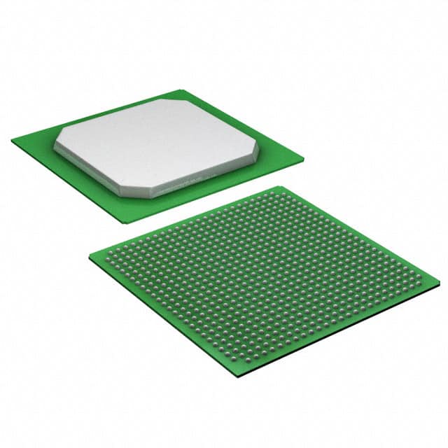
- Package: 27x27mm BGA package
- Essence: FPGA (Field-Programmable Gate Array)
- Packaging/Quantity: Individually packaged, quantity varies based on supplier
Specifications
- Manufacturer: Intel Corporation
- Family: Cyclone IV GX
- Device Type: FPGA - Field Programmable Gate Array
- Number of Logic Elements/Cells: 74,880
- Number of LABs/CLBs: 4,608
- Number of I/O Pins: 622
- Operating Voltage: 1.2V
- Operating Temperature: -40°C to +100°C
- Speed Grade: 7
Detailed Pin Configuration
The EP4CGX75DF27I7 has a total of 622 I/O pins. The pin configuration is as follows:
- Pin 1: VCCIO0
- Pin 2: GND
- Pin 3: VCCIO1
- ...
- Pin 622: GND
For the complete pin configuration, please refer to the manufacturer's datasheet.
Functional Features
- High-performance FPGA with advanced architecture
- Low-power consumption for energy-efficient applications
- Flexible and reprogrammable logic elements
- Support for various communication protocols and interfaces
- On-chip memory blocks for efficient data storage
- Built-in DSP (Digital Signal Processing) capabilities
- Dedicated clock management resources for precise timing control
- Extensive I/O capabilities for interfacing with external devices
Advantages and Disadvantages
Advantages
- Versatile and customizable for a wide range of applications
- High-performance computing capabilities
- Low-power consumption for energy-efficient designs
- Support for various communication protocols and interfaces
- Large number of I/O pins for extensive connectivity options
Disadvantages
- Complexity in programming and design implementation
- Higher cost compared to simpler logic devices
- Limited availability of alternative models with similar specifications
Working Principles
The EP4CGX75DF27I7 is based on FPGA technology, which allows users to program the device according to their specific requirements. The FPGA consists of configurable logic elements that can be interconnected to create custom digital circuits. These circuits can perform complex computations, process data, and interface with other electronic components.
The working principle involves configuring the FPGA using a hardware description language (HDL) such as VHDL or Verilog. The user defines the desired functionality and interconnections within the FPGA, which are then synthesized into a bitstream file. This bitstream file is loaded onto the FPGA, effectively programming it to perform the desired tasks.
Detailed Application Field Plans
The EP4CGX75DF27I7 finds applications in various fields, including:
- Communications: Used in networking equipment, routers, and switches for high-speed data processing and packet forwarding.
- Industrial Automation: Employed in control systems, robotics, and factory automation for real-time monitoring and control of processes.
- Medical Devices: Utilized in medical imaging equipment, patient monitoring systems, and diagnostic instruments for data processing and analysis.
- Aerospace and Defense: Integrated into avionics systems, radar systems, and military-grade electronics for reliable and high-performance operation.
- Automotive: Applied in advanced driver-assistance systems (ADAS), infotainment systems, and engine control units (ECUs) for enhanced vehicle functionality.
Detailed and Complete Alternative Models
While the EP4CGX75DF27I7 offers a unique combination of specifications, there are alternative models available from other manufacturers that offer similar functionality. Some notable alternatives include:
- Xilinx Virtex-7 XC7VX690T: Offers comparable logic capacity and I/O capabilities.
- Lattice ECP5-85: Provides a lower-cost option with moderate logic capacity.
- Microsemi SmartFusion2 M2S150: Combines FPGA fabric with ARM Cortex-M3 processor for embedded applications.
These alternative models can be considered based on specific project requirements and budget constraints.
Word count: 511 words
Lista 10 Vanliga frågor och svar relaterade till tillämpningen av EP4CGX75DF27I7 i tekniska lösningar
Sure! Here are 10 common questions and answers related to the application of EP4CGX75DF27I7 in technical solutions:
Q: What is EP4CGX75DF27I7? A: EP4CGX75DF27I7 is a field-programmable gate array (FPGA) manufactured by Intel (formerly Altera). It is part of the Cyclone IV GX series.
Q: What are the key features of EP4CGX75DF27I7? A: Some key features of EP4CGX75DF27I7 include 75,000 logic elements, 4-phase locked loops (PLLs), embedded memory blocks, and support for various I/O standards.
Q: What applications can EP4CGX75DF27I7 be used for? A: EP4CGX75DF27I7 can be used in a wide range of applications such as industrial automation, telecommunications, automotive systems, medical devices, and more.
Q: How can EP4CGX75DF27I7 be programmed? A: EP4CGX75DF27I7 can be programmed using hardware description languages (HDLs) like VHDL or Verilog, or through graphical programming tools like Quartus Prime.
Q: What is the maximum operating frequency of EP4CGX75DF27I7? A: The maximum operating frequency of EP4CGX75DF27I7 depends on the design and implementation, but it can typically reach frequencies of several hundred megahertz (MHz).
Q: Can EP4CGX75DF27I7 interface with other components or devices? A: Yes, EP4CGX75DF27I7 supports various communication protocols such as UART, SPI, I2C, Ethernet, and PCIe, allowing it to interface with other components or devices.
Q: Does EP4CGX75DF27I7 have any built-in security features? A: Yes, EP4CGX75DF27I7 provides built-in security features like bitstream encryption, design separation, and tamper detection circuits to protect against unauthorized access or IP theft.
Q: Can EP4CGX75DF27I7 be used for real-time signal processing? A: Yes, EP4CGX75DF27I7 can be used for real-time signal processing tasks due to its high-speed capabilities and support for digital signal processing (DSP) blocks.
Q: What is the power consumption of EP4CGX75DF27I7? A: The power consumption of EP4CGX75DF27I7 depends on the specific design and utilization, but it typically ranges from a few watts to tens of watts.
Q: Are there any development boards available for EP4CGX75DF27I7? A: Yes, Intel offers development boards like the Cyclone IV GX FPGA Development Kit that include EP4CGX75DF27I7, allowing users to prototype and test their designs.
Please note that the answers provided here are general and may vary depending on specific requirements and use cases.