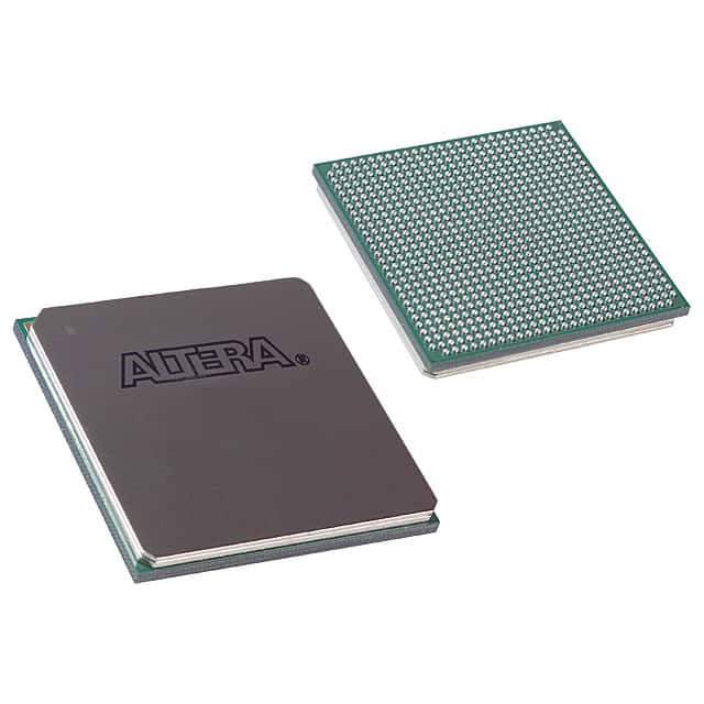
EP4CE75F29C8N
Product Overview
Category
EP4CE75F29C8N belongs to the category of Field Programmable Gate Arrays (FPGAs).
Use
This product is widely used in various electronic applications that require high-speed processing and reconfigurability.
Characteristics
- High-performance FPGA with advanced features
- Offers a large number of logic elements and memory blocks
- Provides flexible and customizable digital circuitry
- Supports complex algorithms and data processing tasks
- Enables rapid prototyping and system development
Package
EP4CE75F29C8N is available in a compact and durable package, ensuring easy integration into electronic systems.
Essence
The essence of EP4CE75F29C8N lies in its ability to provide a versatile and programmable hardware platform for implementing complex digital designs.
Packaging/Quantity
This product is typically packaged in trays or reels, with each containing a specific quantity of EP4CE75F29C8N units. The exact packaging and quantity may vary depending on the manufacturer.
Specifications
- Logic Elements: 75,000
- Memory Blocks: 2,520
- Maximum User I/Os: 531
- Clock Management: PLLs and DLLs
- Operating Voltage: 1.2V
- Operating Temperature Range: -40°C to 100°C
- Package Type: BGA (Ball Grid Array)
- Package Pins: 780
Detailed Pin Configuration
For a detailed pin configuration diagram and description, please refer to the official datasheet provided by the manufacturer.
Functional Features
EP4CE75F29C8N offers several functional features that make it a preferred choice for various applications:
High-Speed Processing: The FPGA provides fast data processing capabilities, enabling real-time operations in demanding applications.
Reconfigurability: EP4CE75F29C8N allows users to modify the hardware configuration, making it adaptable to changing requirements without the need for physical changes.
Flexible I/O Interfaces: The product supports a wide range of input and output interfaces, facilitating seamless integration with other electronic components.
Embedded Memory: With a large number of memory blocks, this FPGA can efficiently store and retrieve data during processing tasks.
Clock Management: The built-in PLLs and DLLs ensure precise clock generation and distribution, enabling synchronization of various components within the system.
Advantages and Disadvantages
Advantages
- High-performance and reconfigurable platform
- Supports complex algorithms and data processing tasks
- Enables rapid prototyping and system development
- Flexible I/O interfaces for seamless integration
- Precise clock management for synchronization
Disadvantages
- Relatively high power consumption compared to other programmable logic devices
- Steeper learning curve for beginners due to its complexity
Working Principles
EP4CE75F29C8N operates based on the principles of digital logic design. It consists of configurable logic elements, memory blocks, and I/O interfaces. Users can program the FPGA using Hardware Description Languages (HDL) such as VHDL or Verilog. Once programmed, the FPGA executes the desired digital circuitry by routing signals through the configurable logic elements and memory blocks.
Detailed Application Field Plans
EP4CE75F29C8N finds applications in various fields, including:
- Communications: Used in wireless communication systems, network routers, and base stations for signal processing and protocol implementation.
- Industrial Automation: Employed in control systems, robotics, and machine vision applications for real-time data processing and control.
- Medical Electronics: Utilized in medical imaging devices, patient monitoring systems, and diagnostic equipment for high-speed data processing and analysis.
- Automotive: Integrated into advanced driver assistance systems (ADAS), infotainment systems, and engine control units for efficient data processing and control.
- Aerospace and Defense: Used in radar systems, avionics, and military communication systems for high-performance signal processing and encryption.
Detailed and Complete Alternative Models
- Altera Cyclone IV EP4CE115F29C8N
- Xilinx Spartan-6 XC6SLX75T-3FGG484C
- Lattice ECP5-85F-6BG256C
These alternative models offer similar functionality and performance to EP4CE75F29C8N and can be considered as alternatives based on specific project requirements.
Note: The content provided above is an overview and should be supplemented with the official datasheet and technical documentation for a comprehensive understanding of EP4CE75F29C8N.
Lista 10 Vanliga frågor och svar relaterade till tillämpningen av EP4CE75F29C8N i tekniska lösningar
Sure! Here are 10 common questions and answers related to the application of EP4CE75F29C8N in technical solutions:
Q: What is EP4CE75F29C8N? A: EP4CE75F29C8N is a field-programmable gate array (FPGA) manufactured by Intel (formerly Altera). It offers a range of programmable logic elements and embedded memory blocks.
Q: What are the key features of EP4CE75F29C8N? A: Some key features include 75,000 logic elements, 29,040 adaptive logic modules, 8,352 embedded memory blocks, and support for various I/O standards.
Q: What are the typical applications of EP4CE75F29C8N? A: EP4CE75F29C8N is commonly used in applications such as digital signal processing, high-speed communication systems, industrial automation, robotics, and image/video processing.
Q: How can EP4CE75F29C8N be programmed? A: EP4CE75F29C8N can be programmed using hardware description languages (HDLs) like VHDL or Verilog, or through graphical programming tools like Quartus Prime.
Q: Can EP4CE75F29C8N interface with other components or devices? A: Yes, EP4CE75F29C8N supports various communication protocols such as UART, SPI, I2C, Ethernet, and PCIe, allowing it to interface with a wide range of components and devices.
Q: What kind of development board is compatible with EP4CE75F29C8N? A: The DE0-Nano development board is commonly used with EP4CE75F29C8N, providing a platform for prototyping and testing FPGA-based designs.
Q: Can EP4CE75F29C8N be used in safety-critical applications? A: Yes, EP4CE75F29C8N can be used in safety-critical applications, but additional measures such as redundancy and fault-tolerant design techniques may be required to ensure reliability.
Q: What are the power requirements for EP4CE75F29C8N? A: The typical operating voltage for EP4CE75F29C8N is 1.2V, but it also requires additional voltages for I/O banks and configuration pins, which can vary depending on the application.
Q: Is there any documentation available for EP4CE75F29C8N? A: Yes, Intel provides comprehensive documentation, including datasheets, user guides, reference manuals, and application notes, which can be found on their website.
Q: Are there any development tools available for programming EP4CE75F29C8N? A: Yes, Intel provides Quartus Prime, a powerful software suite that includes a graphical design environment, synthesis tools, simulation tools, and programming utilities for EP4CE75F29C8N.
Please note that the answers provided here are general and may vary based on specific requirements and use cases. It's always recommended to refer to the official documentation and consult with experts when working with EP4CE75F29C8N or any other technical solution.


