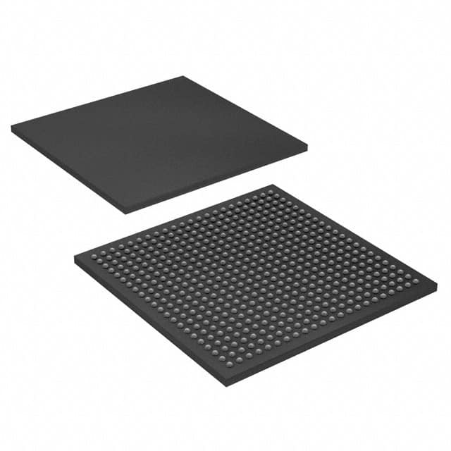
EP3C40U484C7
Product Overview
- Category: Integrated Circuit (IC)
- Use: Programmable Logic Device (PLD)
- Characteristics: High-performance, low-power consumption
- Package: 484-pin BGA (Ball Grid Array)
- Essence: Field-Programmable Gate Array (FPGA)
- Packaging/Quantity: Single unit
Specifications
- Logic Elements: 40,000
- Embedded Memory: 1,152 Kbits
- Maximum User I/Os: 317
- Operating Voltage: 1.2V
- Operating Temperature: -40°C to 100°C
- Speed Grade: 7
Detailed Pin Configuration
The EP3C40U484C7 has a total of 484 pins, each serving a specific purpose in the device's functionality. The pin configuration includes input/output pins, power supply pins, ground pins, and configuration pins. A detailed pinout diagram can be found in the product datasheet.
Functional Features
- High Performance: The EP3C40U484C7 offers high-speed operation and efficient logic utilization, making it suitable for demanding applications.
- Low Power Consumption: With its advanced power management features, the device minimizes power consumption while maintaining optimal performance.
- Flexibility: Being a field-programmable device, the EP3C40U484C7 allows users to configure and reconfigure its internal logic according to their specific requirements.
- Versatility: The FPGA architecture enables the implementation of various digital functions, including complex algorithms, data processing, and control systems.
Advantages and Disadvantages
Advantages: - Customizable: The EP3C40U484C7 can be tailored to meet specific application needs. - Rapid Prototyping: The FPGA's reprogrammability allows for quick iterations during the development phase. - High Integration: The device combines multiple functions into a single chip, reducing system complexity and cost.
Disadvantages: - Complexity: Designing and programming an FPGA requires specialized knowledge and expertise. - Cost: FPGAs tend to be more expensive than fixed-function integrated circuits for large-scale production.
Working Principles
The EP3C40U484C7 is based on the Field-Programmable Gate Array (FPGA) technology. It consists of an array of configurable logic blocks interconnected through programmable interconnects. The device can be programmed using Hardware Description Languages (HDLs) such as VHDL or Verilog, which define the desired functionality and interconnections within the FPGA.
During operation, the EP3C40U484C7 executes the configured logic functions by routing signals through the programmable interconnects and logic blocks. This allows for the implementation of complex digital circuits, including arithmetic operations, data storage, and control functions.
Detailed Application Field Plans
The EP3C40U484C7 finds applications in various fields, including:
- Communications: Used in networking equipment, routers, and switches for high-speed data processing and protocol handling.
- Industrial Automation: Employed in control systems, robotics, and machine vision applications for real-time control and image processing.
- Medical Devices: Utilized in medical imaging, patient monitoring, and diagnostic equipment for signal processing and data analysis.
- Aerospace and Defense: Integrated into avionics systems, radar processing, and secure communication systems for reliable and high-performance operation.
- Consumer Electronics: Found in smart TVs, gaming consoles, and multimedia devices for video and audio processing.
Alternative Models
In addition to the EP3C40U484C7, there are alternative models available in the market that offer similar functionality and performance. Some notable alternatives include:
- EP3C25F324C8: A smaller FPGA with 25,000 logic elements and 324-pin package.
- EP4CE115F29C7: A higher-end FPGA with 115,000 logic elements and 484-pin package.
- XC7A35T-1CPG236C: An FPGA from a different manufacturer, offering 35,000 logic cells and 236-pin package.
These alternative models provide options for users based on their specific requirements and project constraints.
Word count: 529 words
Lista 10 Vanliga frågor och svar relaterade till tillämpningen av EP3C40U484C7 i tekniska lösningar
Sure! Here are 10 common questions and answers related to the application of EP3C40U484C7 in technical solutions:
Q: What is EP3C40U484C7? A: EP3C40U484C7 is a specific model of Field-Programmable Gate Array (FPGA) manufactured by Altera.
Q: What are the key features of EP3C40U484C7? A: EP3C40U484C7 offers 40,000 logic elements, 1,288 Kbits of embedded memory, and various I/O interfaces for versatile applications.
Q: What are some typical applications of EP3C40U484C7? A: EP3C40U484C7 is commonly used in digital signal processing, industrial automation, telecommunications, and high-performance computing applications.
Q: How can EP3C40U484C7 be programmed? A: EP3C40U484C7 can be programmed using Hardware Description Languages (HDLs) such as VHDL or Verilog, along with design software like Quartus Prime.
Q: Can EP3C40U484C7 be reprogrammed after deployment? A: Yes, EP3C40U484C7 is a reprogrammable FPGA, allowing for flexibility and iterative development.
Q: What are the power requirements for EP3C40U484C7? A: EP3C40U484C7 typically operates at a voltage range of 1.15V to 1.25V, with additional power supply pins for different components.
Q: Does EP3C40U484C7 support external memory interfaces? A: Yes, EP3C40U484C7 supports various external memory interfaces like DDR3, DDR2, and QDR II+ for efficient data storage and retrieval.
Q: Can EP3C40U484C7 interface with other devices or protocols? A: Yes, EP3C40U484C7 offers multiple I/O standards, including LVDS, PCI Express, Ethernet, and USB, enabling seamless integration with other devices.
Q: Are there any development boards available for EP3C40U484C7? A: Yes, Altera provides development boards like the Cyclone III Starter Kit, which includes EP3C40U484C7, allowing for rapid prototyping and evaluation.
Q: Where can I find technical documentation and support for EP3C40U484C7? A: You can find detailed technical documentation, datasheets, reference designs, and support resources on the official Altera/Intel FPGA website.


