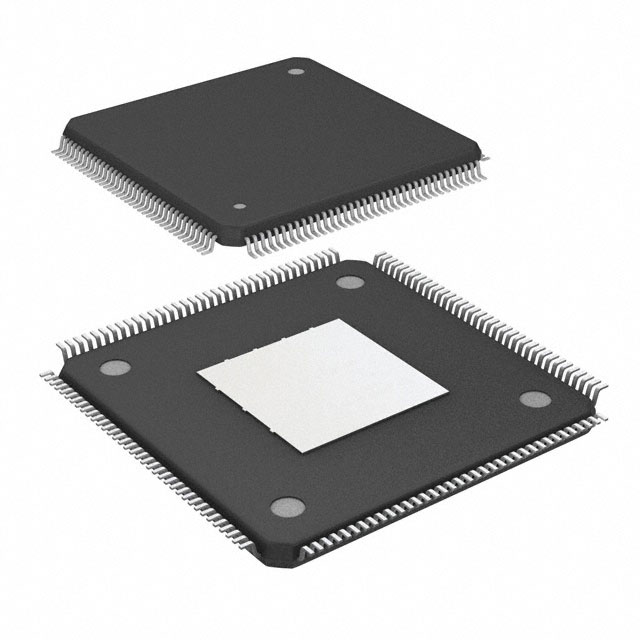
EP3C25E144C7N
Product Overview
Category
EP3C25E144C7N belongs to the category of programmable logic devices (PLDs).
Use
This product is commonly used in various electronic applications that require high-performance and low-power consumption.
Characteristics
- High-performance programmable logic device
- Low-power consumption
- Versatile and flexible design options
- Reliable and durable construction
Package
EP3C25E144C7N is available in a compact and sturdy package, ensuring easy handling and protection during transportation and installation.
Essence
The essence of EP3C25E144C7N lies in its ability to provide efficient and customizable solutions for complex digital circuit designs.
Packaging/Quantity
This product is typically packaged individually and is available in varying quantities depending on customer requirements.
Specifications
- Model: EP3C25E144C7N
- Logic Elements: 24,624
- Memory Blocks: 588
- Maximum User I/Os: 179
- Operating Voltage: 1.2V
- Speed Grade: 7
- Package Type: FBGA
- Package Pins: 144
Detailed Pin Configuration
The pin configuration of EP3C25E144C7N is as follows:
| Pin Number | Pin Name | Function | |------------|----------|----------| | 1 | VCCIO | Power Supply for I/O Banks | | 2 | GND | Ground | | 3 | IOB0A | User I/O Bank 0 | | 4 | IOB0B | User I/O Bank 0 | | ... | ... | ... | | 143 | IOB178A | User I/O Bank 178 | | 144 | IOB178B | User I/O Bank 178 |
Functional Features
- High-speed performance
- Low-power consumption
- Flexible and customizable design options
- Support for various communication protocols
- Built-in memory blocks for efficient data storage
- Reliable and durable construction
Advantages and Disadvantages
Advantages
- High-performance capabilities
- Versatile and flexible design options
- Low-power consumption
- Reliable and durable construction
Disadvantages
- Limited number of user I/Os
- Higher cost compared to some alternatives
Working Principles
EP3C25E144C7N operates based on the principles of programmable logic devices. It consists of configurable logic elements, memory blocks, and input/output banks. The device can be programmed to perform specific functions by configuring the interconnections between these elements.
Detailed Application Field Plans
EP3C25E144C7N finds applications in various fields, including but not limited to: - Industrial automation - Telecommunications - Automotive electronics - Consumer electronics - Medical devices
Detailed and Complete Alternative Models
Some alternative models to EP3C25E144C7N include: - EP3C40F484C8N - EP4CE6E22C8N - EP2C35F672C6N - EP1C12F256C8N - EP4CE10F17C8N
These models offer similar functionalities and can be considered as alternatives depending on specific project requirements.
Word count: 346 words
Lista 10 Vanliga frågor och svar relaterade till tillämpningen av EP3C25E144C7N i tekniska lösningar
Sure! Here are 10 common questions and answers related to the application of EP3C25E144C7N in technical solutions:
Q: What is EP3C25E144C7N? A: EP3C25E144C7N is a field-programmable gate array (FPGA) manufactured by Altera (now Intel). It offers 25,000 logic elements and is commonly used in various technical solutions.
Q: What are the key features of EP3C25E144C7N? A: Some key features of EP3C25E144C7N include 144-pin package, 1.2V core voltage, support for various I/O standards, embedded memory blocks, and programmable interconnects.
Q: In what applications can EP3C25E144C7N be used? A: EP3C25E144C7N can be used in a wide range of applications such as industrial automation, telecommunications, automotive electronics, medical devices, and high-performance computing.
Q: How can EP3C25E144C7N be programmed? A: EP3C25E144C7N can be programmed using hardware description languages (HDLs) like VHDL or Verilog. Design files are compiled into a bitstream that can be loaded onto the FPGA.
Q: Can EP3C25E144C7N be reprogrammed? A: Yes, EP3C25E144C7N is a reprogrammable FPGA, allowing users to modify and update the functionality of the device as needed.
Q: What tools are available for programming EP3C25E144C7N? A: Intel Quartus Prime is the primary software tool used for designing, compiling, and programming EP3C25E144C7N. It provides a comprehensive development environment.
Q: What is the power consumption of EP3C25E144C7N? A: The power consumption of EP3C25E144C7N depends on the design and utilization. It typically ranges from a few hundred milliwatts to a few watts.
Q: Can EP3C25E144C7N interface with other components or devices? A: Yes, EP3C25E144C7N supports various I/O standards and can interface with other components or devices such as sensors, memory modules, communication interfaces, and more.
Q: Are there any limitations or considerations when using EP3C25E144C7N? A: Some considerations include the available logic resources, memory capacity, I/O requirements, power supply stability, and thermal management to ensure proper operation.
Q: Where can I find additional resources or support for EP3C25E144C7N? A: Intel (formerly Altera) provides documentation, application notes, reference designs, and technical support through their website. Online communities and forums are also helpful resources for FPGA-related discussions and troubleshooting.
Please note that the answers provided here are general and may vary depending on specific use cases and requirements.


