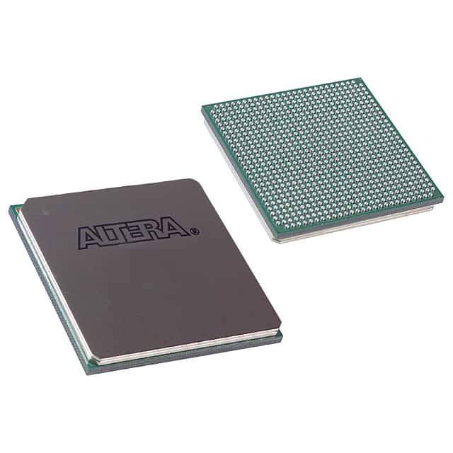
EP2SGX30DF780C5
Product Overview
- Category: Integrated Circuit (IC)
- Use: Programmable Logic Device (PLD)
- Characteristics: High-performance, low-power consumption
- Package: 780-pin FineLine BGA package
- Essence: FPGA (Field-Programmable Gate Array)
- Packaging/Quantity: Single unit
Specifications
- Manufacturer: Intel Corporation
- Family: Stratix II GX
- Device: EP2SGX30DF780C5
- Technology: 90nm
- Logic Elements: 29,040
- Embedded Multipliers: 288
- Maximum User I/Os: 622
- Operating Voltage: 1.2V
- Operating Temperature: -40°C to +100°C
Detailed Pin Configuration
The EP2SGX30DF780C5 has a total of 780 pins arranged in a specific configuration. The pinout diagram and detailed pin descriptions can be found in the manufacturer's datasheet.
Functional Features
- High-speed performance: The EP2SGX30DF780C5 offers fast logic processing capabilities, making it suitable for applications that require real-time data processing.
- Low power consumption: This PLD is designed to minimize power usage, making it energy-efficient and suitable for battery-powered devices.
- Flexible reprogrammability: The FPGA nature of the device allows users to modify its functionality by reprogramming it, providing flexibility for various applications.
- Ample I/O capabilities: With 622 user I/Os, the EP2SGX30DF780C5 provides sufficient connectivity options for interfacing with external devices.
Advantages and Disadvantages
Advantages: - High-performance processing - Low power consumption - Reprogrammable nature - Ample I/O capabilities
Disadvantages: - Limited logic elements compared to higher-end models - Higher cost compared to lower-capacity alternatives
Working Principles
The EP2SGX30DF780C5 is based on FPGA technology, which consists of an array of configurable logic blocks interconnected through programmable interconnects. These logic blocks can be programmed to perform various functions, allowing the device to implement complex digital circuits. The configuration of the logic blocks and interconnects is stored in internal memory cells, which can be reprogrammed as needed.
Detailed Application Field Plans
The EP2SGX30DF780C5 is suitable for a wide range of applications, including but not limited to: - High-speed data processing systems - Digital signal processing (DSP) - Image and video processing - Communication systems - Industrial automation - Aerospace and defense applications
Detailed and Complete Alternative Models
- EP2SGX15DF780C5: Lower capacity version with 14,080 logic elements and 144 embedded multipliers.
- EP2SGX50DF780C5: Higher capacity version with 49,680 logic elements and 396 embedded multipliers.
- EP2SGX100DF780C5: Higher capacity version with 99,360 logic elements and 792 embedded multipliers.
These alternative models provide different levels of logic capacity and are suitable for various application requirements.
Word count: 314 words
Lista 10 Vanliga frågor och svar relaterade till tillämpningen av EP2SGX30DF780C5 i tekniska lösningar
Sure! Here are 10 common questions and answers related to the application of EP2SGX30DF780C5 in technical solutions:
Q: What is EP2SGX30DF780C5? A: EP2SGX30DF780C5 is a specific model of field-programmable gate array (FPGA) manufactured by Intel.
Q: What are the key features of EP2SGX30DF780C5? A: Some key features of EP2SGX30DF780C5 include high logic density, high-speed transceivers, embedded memory blocks, and support for various I/O standards.
Q: In what applications can EP2SGX30DF780C5 be used? A: EP2SGX30DF780C5 can be used in a wide range of applications such as telecommunications, networking, industrial automation, aerospace, and defense.
Q: How does EP2SGX30DF780C5 differ from other FPGAs? A: EP2SGX30DF780C5 offers higher logic density and more advanced features compared to some other FPGAs, making it suitable for complex and demanding applications.
Q: What development tools are available for EP2SGX30DF780C5? A: Intel provides Quartus Prime software suite, which includes design entry, synthesis, simulation, and programming tools specifically tailored for EP2SGX30DF780C5.
Q: Can EP2SGX30DF780C5 be reprogrammed after deployment? A: Yes, EP2SGX30DF780C5 is a reprogrammable FPGA, allowing users to modify its functionality even after it has been deployed in a system.
Q: What is the power consumption of EP2SGX30DF780C5? A: The power consumption of EP2SGX30DF780C5 depends on the specific design and usage scenario, but it typically falls within a certain range specified in the datasheet.
Q: Does EP2SGX30DF780C5 support high-speed serial communication? A: Yes, EP2SGX30DF780C5 has built-in high-speed transceivers that support various protocols like PCIe, Ethernet, and USB.
Q: Can EP2SGX30DF780C5 interface with external memory devices? A: Yes, EP2SGX30DF780C5 has embedded memory blocks and also supports external memory interfaces like DDR3 or DDR4 SDRAM.
Q: Are there any reference designs or application notes available for EP2SGX30DF780C5? A: Yes, Intel provides reference designs and application notes to help users get started with EP2SGX30DF780C5 and implement specific functionalities efficiently.
Please note that the answers provided here are general and may vary depending on the specific requirements and use cases. It is always recommended to refer to the official documentation and datasheets for accurate and up-to-date information.


