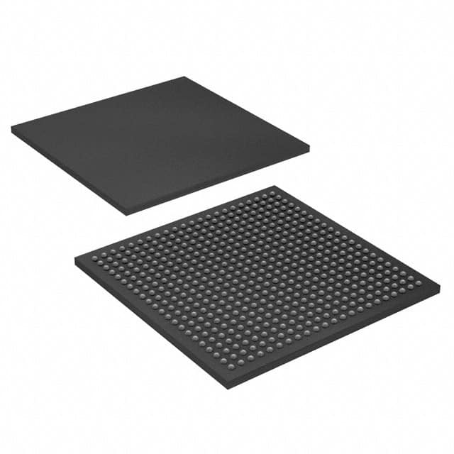
EP2C35F484I8
Product Overview
Category: Integrated Circuit (IC)
Use: EP2C35F484I8 is a programmable logic device (PLD) that belongs to the Cyclone II family of Field-Programmable Gate Arrays (FPGAs). It is designed for various applications in industries such as telecommunications, automotive, consumer electronics, and industrial automation.
Characteristics: - High-performance FPGA with low power consumption - Offers high-speed data processing capabilities - Provides flexibility for customization and reconfiguration - Supports a wide range of I/O interfaces - Can be programmed using hardware description languages (HDLs) like VHDL or Verilog
Package: The EP2C35F484I8 comes in a 484-pin FineLine BGA (Ball Grid Array) package. This package provides a compact form factor and allows for efficient heat dissipation.
Essence: EP2C35F484I8 is a key component in electronic systems that require high-speed data processing and flexible functionality. It enables designers to implement complex digital circuits and algorithms in a single chip.
Packaging/Quantity: The EP2C35F484I8 is typically sold individually or in reels containing multiple units, depending on the supplier. The exact quantity may vary based on the manufacturer's packaging standards.
Specifications
- Logic Elements: 33,216
- Total RAM Bits: 1,048,576
- Maximum User I/O Pins: 317
- Maximum User Flash Memory: 4,608 Kbits
- Clock Networks: 4
- PLLs (Phase-Locked Loops): 2
- Maximum Operating Frequency: 300 MHz
- Operating Voltage: 1.2V
Detailed Pin Configuration
The EP2C35F484I8 has a total of 484 pins, each serving a specific purpose in the device's operation. The pin configuration includes power supply pins, ground pins, I/O pins, clock pins, and configuration pins. A detailed pinout diagram can be found in the device's datasheet.
Functional Features
- High-speed data processing: EP2C35F484I8 offers fast logic operations and efficient data handling capabilities.
- Flexible configuration: The device can be programmed and reprogrammed to implement various digital circuits and algorithms.
- Extensive I/O support: It supports a wide range of I/O standards, enabling seamless integration with other components.
- Low power consumption: EP2C35F484I8 is designed to minimize power consumption while maintaining high performance.
- On-chip memory: The device includes embedded memory blocks for storing data during operation.
Advantages and Disadvantages
Advantages: - Versatile and customizable: EP2C35F484I8 allows designers to create tailored solutions for different applications. - High-performance capabilities: The FPGA offers fast data processing and efficient resource utilization. - Cost-effective: Programmable logic devices eliminate the need for custom ASICs, reducing development costs.
Disadvantages: - Complexity: Working with FPGAs requires expertise in hardware description languages and digital design. - Limited resources: The available logic elements, memory, and I/O pins may impose constraints on complex designs. - Power consumption: While efforts have been made to reduce power consumption, FPGAs still consume more power compared to dedicated ASICs.
Working Principles
EP2C35F484I8 operates based on the principles of field-programmable gate arrays. It consists of configurable logic blocks (CLBs), interconnect resources, I/O elements, and embedded memory blocks. The device can be programmed using HDLs, which describe the desired functionality and interconnections of the digital circuit. Once programmed, the FPGA executes the specified logic operations and data processing tasks.
Detailed Application Field Plans
EP2C35F484I8 finds applications in various fields, including:
- Telecommunications: Used in network routers, switches, and base stations for high-speed data processing and protocol handling.
- Automotive: Employed in automotive control systems, infotainment systems, and driver assistance systems for real-time data processing and control.
- Consumer Electronics: Utilized in smart TVs, set-top boxes, and gaming consoles for multimedia processing and user interface control.
- Industrial Automation: Integrated into industrial control systems, robotics, and factory automation equipment for precise control and monitoring.
Detailed and Complete Alternative Models
- EP2C20F484I8: A lower-capacity variant of the same Cyclone II FPGA family, suitable for less demanding applications.
- EP4CE115F29C7: A higher-capacity FPGA from Altera's Cyclone IV series, offering increased logic elements and I/O pins.
- XC7A35T-1CPG236C: A Xilinx Artix-7 FPGA with similar capabilities, providing
Lista 10 Vanliga frågor och svar relaterade till tillämpningen av EP2C35F484I8 i tekniska lösningar
Sure! Here are 10 common questions and answers related to the application of EP2C35F484I8 in technical solutions:
Q: What is EP2C35F484I8? A: EP2C35F484I8 is a field-programmable gate array (FPGA) manufactured by Intel. It is commonly used in various technical solutions for its versatility and programmability.
Q: What are the key features of EP2C35F484I8? A: Some key features of EP2C35F484I8 include 35,200 logic elements, 1,288 embedded memory blocks, 4 PLLs, and support for various I/O standards.
Q: What applications can EP2C35F484I8 be used for? A: EP2C35F484I8 can be used in a wide range of applications such as digital signal processing, image and video processing, communication systems, industrial automation, and more.
Q: How do I program EP2C35F484I8? A: EP2C35F484I8 can be programmed using hardware description languages (HDLs) like VHDL or Verilog, which describe the desired functionality of the FPGA. The programming file is then loaded onto the FPGA using a programmer.
Q: Can EP2C35F484I8 be reprogrammed? A: Yes, EP2C35F484I8 is a reprogrammable FPGA. You can modify the design and reprogram it multiple times to suit different requirements.
Q: What development tools are available for EP2C35F484I8? A: Intel provides Quartus Prime software, which includes a suite of development tools for designing, simulating, and programming EP2C35F484I8.
Q: What is the power supply requirement for EP2C35F484I8? A: EP2C35F484I8 typically requires a 3.3V power supply, but it also has built-in voltage regulators to support different I/O standards.
Q: Can EP2C35F484I8 interface with other components or devices? A: Yes, EP2C35F484I8 supports various communication interfaces like UART, SPI, I2C, and Ethernet, allowing it to interface with other components or devices in a system.
Q: Are there any limitations or considerations when using EP2C35F484I8? A: Some considerations include power consumption, heat dissipation, and timing constraints. It's important to carefully design and optimize your FPGA implementation to meet these requirements.
Q: Where can I find additional resources and support for EP2C35F484I8? A: Intel provides documentation, application notes, reference designs, and an online community forum where you can find additional resources and get support for EP2C35F484I8.


