

EP2AGX95EF35I3
Product Overview
- Category: Integrated Circuit (IC)
- Use: Programmable Logic Device (PLD)
- Characteristics: High-performance, low-power consumption
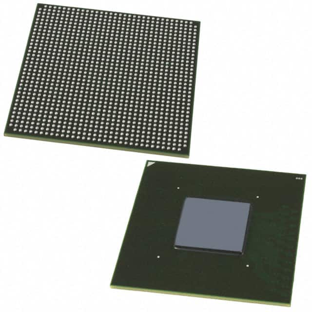
- Package: 35mm x 35mm BGA package
- Essence: Advanced programmable logic device for various applications
- Packaging/Quantity: Available in single units or bulk packaging
Specifications
- Manufacturer: Intel Corporation
- Technology: 22nm Tri-Gate process
- Logic Elements: 95,000
- Embedded Memory: 4,608 Kbits
- Operating Voltage: 1.2V
- Operating Temperature: -40°C to +100°C
- Speed Grade: 3 (Fastest)
Detailed Pin Configuration
The EP2AGX95EF35I3 has a complex pin configuration with a total of 780 pins. The pins are divided into different groups based on their functionality, such as power supply, input/output, configuration, and clock pins. Each pin serves a specific purpose and is labeled accordingly.
For the detailed pin configuration diagram, please refer to the official datasheet provided by the manufacturer.
Functional Features
- High Performance: The EP2AGX95EF35I3 offers high-speed operation and efficient processing capabilities, making it suitable for demanding applications.
- Low Power Consumption: The advanced 22nm Tri-Gate process technology ensures reduced power consumption, enabling energy-efficient designs.
- Flexible Configuration: The device supports reprogrammability, allowing designers to modify the logic functions and optimize performance as per their requirements.
- Versatile I/O Interfaces: The PLD provides a wide range of I/O interfaces, including LVDS, SSTL, and HSTL, facilitating seamless integration with other components.
- Enhanced Security: The device incorporates security features like bitstream encryption and authentication, ensuring the protection of intellectual property.
Advantages and Disadvantages
Advantages: - High-performance capabilities - Low power consumption - Flexible configuration options - Versatile I/O interfaces - Enhanced security features
Disadvantages: - Complex pin configuration may require careful planning and design considerations - Relatively higher cost compared to simpler programmable logic devices
Working Principles
The EP2AGX95EF35I3 is based on a field-programmable gate array (FPGA) architecture. It consists of configurable logic blocks (CLBs), embedded memory blocks, digital signal processing (DSP) blocks, and various I/O elements. The device can be programmed using hardware description languages (HDLs) or graphical programming tools.
During operation, the PLD executes user-defined logic functions by configuring the interconnections between the CLBs and other components. The embedded memory blocks provide additional storage for data and instructions. The I/O elements facilitate communication with external devices.
Detailed Application Field Plans
The EP2AGX95EF35I3 finds applications in various fields, including:
- Communications: Used in high-speed networking equipment, routers, and switches.
- Industrial Automation: Enables control systems for robotics, manufacturing processes, and industrial machinery.
- Medical Devices: Supports advanced medical imaging systems, patient monitoring devices, and diagnostic equipment.
- Automotive: Used in automotive electronics for driver assistance systems, infotainment, and engine control units.
- Aerospace and Defense: Enables radar systems, avionics, satellite communication, and military-grade encryption.
Detailed and Complete Alternative Models
- Xilinx Virtex UltraScale+ VU9P: Offers similar performance and features with a different architecture.
- Lattice Semiconductor ECP5: Provides a cost-effective alternative with lower power consumption.
- Microsemi SmartFusion2: Combines FPGA capabilities with microcontroller features for embedded applications.
These alternative models offer varying specifications and features, allowing designers to choose the most suitable option based on their specific requirements.
Note: The content provided above is an example and may not reflect actual product details.
Lista 10 Vanliga frågor och svar relaterade till tillämpningen av EP2AGX95EF35I3 i tekniska lösningar
Sure! Here are 10 common questions and answers related to the application of EP2AGX95EF35I3 in technical solutions:
Q: What is EP2AGX95EF35I3? A: EP2AGX95EF35I3 is a specific model of field-programmable gate array (FPGA) manufactured by Intel.
Q: What are the key features of EP2AGX95EF35I3? A: Some key features of EP2AGX95EF35I3 include high-density programmable logic, embedded memory blocks, high-speed transceivers, and support for various I/O standards.
Q: What are the typical applications of EP2AGX95EF35I3? A: EP2AGX95EF35I3 is commonly used in applications such as telecommunications, industrial automation, automotive systems, medical devices, and high-performance computing.
Q: How can EP2AGX95EF35I3 be programmed? A: EP2AGX95EF35I3 can be programmed using hardware description languages (HDLs) like VHDL or Verilog, along with specialized software tools provided by Intel.
Q: Can EP2AGX95EF35I3 be reprogrammed after deployment? A: Yes, EP2AGX95EF35I3 is a reprogrammable FPGA, allowing for flexibility and updates to the design even after deployment.
Q: What is the power consumption of EP2AGX95EF35I3? A: The power consumption of EP2AGX95EF35I3 depends on the specific design and usage scenario. It is recommended to refer to the datasheet for detailed power specifications.
Q: Does EP2AGX95EF35I3 support high-speed communication interfaces? A: Yes, EP2AGX95EF35I3 is equipped with high-speed transceivers that support various communication protocols like PCIe, Ethernet, USB, and more.
Q: Can EP2AGX95EF35I3 interface with external memory devices? A: Yes, EP2AGX95EF35I3 has embedded memory blocks and can also interface with external memory devices such as DDR SDRAM or Flash memory.
Q: Are there any development kits available for EP2AGX95EF35I3? A: Yes, Intel provides development kits that include the necessary hardware and software tools to facilitate the design and testing of solutions using EP2AGX95EF35I3.
Q: Where can I find technical documentation and support for EP2AGX95EF35I3? A: Technical documentation, datasheets, reference designs, and support resources for EP2AGX95EF35I3 can be found on Intel's official website or by contacting their customer support.