

EP2AGX125DF25C6N
Product Overview
Category
EP2AGX125DF25C6N belongs to the category of Field Programmable Gate Arrays (FPGAs).
Use
FPGAs are integrated circuits that can be programmed and reprogrammed to perform various digital functions. They are widely used in industries such as telecommunications, automotive, aerospace, and consumer electronics.
Characteristics
- EP2AGX125DF25C6N is a high-performance FPGA with advanced features.
- It offers a large number of logic elements, memory blocks, and I/O pins.
- The device operates at high speeds and supports complex digital designs.
- It provides flexibility for customization and adaptation to specific applications.
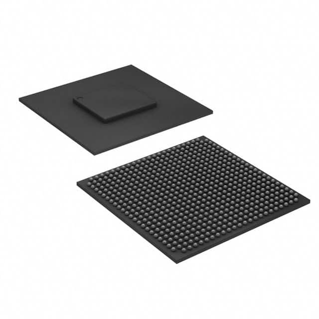
Package
EP2AGX125DF25C6N comes in a compact package designed for easy integration onto printed circuit boards (PCBs). The package ensures proper heat dissipation and protection against environmental factors.
Essence
The essence of EP2AGX125DF25C6N lies in its ability to provide a programmable hardware platform that enables the implementation of complex digital systems. It allows designers to create custom solutions without the need for dedicated application-specific integrated circuits (ASICs).
Packaging/Quantity
EP2AGX125DF25C6N is typically sold in trays or reels containing multiple units. The exact quantity may vary depending on the supplier and customer requirements.
Specifications
- Logic Elements: 125,000
- Memory Blocks: 4,608
- Maximum Operating Frequency: 500 MHz
- I/O Pins: 622
- Power Supply Voltage: 1.2V
- Package Type: FBGA (Fine-pitch Ball Grid Array)
- Package Dimensions: 25mm x 25mm
Detailed Pin Configuration
The pin configuration of EP2AGX125DF25C6N is as follows:
- Pin 1: VCCIO
- Pin 2: GND
- Pin 3: IO0
- Pin 4: IO1
- ...
- Pin 622: IO621
For a complete pin configuration diagram, please refer to the datasheet provided by the manufacturer.
Functional Features
EP2AGX125DF25C6N offers several functional features that enhance its performance and versatility:
- High-Speed Interfaces: The FPGA supports various high-speed interfaces such as PCIe, DDR3, and Ethernet, enabling seamless integration with other components.
- Embedded Memory: The device includes on-chip memory blocks that can be used for data storage or as lookup tables for implementing complex logic functions.
- DSP Blocks: EP2AGX125DF25C6N incorporates dedicated digital signal processing (DSP) blocks, allowing efficient implementation of algorithms requiring high computational power.
- Configuration Options: The FPGA supports multiple configuration modes, including serial and parallel programming, providing flexibility in system design and updates.
Advantages and Disadvantages
Advantages
- Flexibility: EP2AGX125DF25C6N allows designers to create custom digital systems tailored to specific requirements.
- Time-to-Market: FPGAs enable rapid prototyping and development cycles, reducing time-to-market for new products.
- Cost-Effectiveness: Compared to ASICs, FPGAs offer a more cost-effective solution for low to medium volume production runs.
- Reconfigurability: The ability to reprogram the FPGA allows for system upgrades and modifications without hardware changes.
Disadvantages
- Power Consumption: FPGAs generally consume more power compared to fixed-function integrated circuits.
- Complexity: Designing with FPGAs requires specialized knowledge and expertise, making it more challenging for novice users.
- Limited Performance: While FPGAs provide high flexibility, they may not match the performance of dedicated ASICs for specific applications.
Working Principles
EP2AGX125DF25C6N operates based on the principles of configurable logic. The FPGA consists of a matrix of programmable logic elements interconnected through configurable routing resources. These logic elements can be programmed to implement various digital functions, such as arithmetic operations, memory storage, and control logic. The configuration data is loaded into the FPGA using a programming interface, allowing the device to function according to the desired design.
Detailed Application Field Plans
EP2AGX125DF25C6N finds applications in various fields, including:
- Telecommunications: Used in base stations, routers, and network switches for high-speed data processing and protocol handling.
- Automotive: Employed in advanced driver-assistance systems (ADAS) for real-time image processing, sensor fusion, and vehicle control.
- Aerospace: Utilized in satellite communication systems, radar signal processing, and avionics for reliable and efficient data processing.
- Consumer Electronics: Integrated into smart TVs, gaming consoles, and multimedia devices for video and audio processing, user interface control, and connectivity.
Lista 10 Vanliga frågor och svar relaterade till tillämpningen av EP2AGX125DF25C6N i tekniska lösningar
Sure! Here are 10 common questions and answers related to the application of EP2AGX125DF25C6N in technical solutions:
Q: What is EP2AGX125DF25C6N? A: EP2AGX125DF25C6N is a field-programmable gate array (FPGA) manufactured by Intel. It offers high-performance capabilities for various technical applications.
Q: What are the key features of EP2AGX125DF25C6N? A: Some key features include 125,000 logic elements, 3,888 embedded memory blocks, 4 PLLs, and support for various I/O standards.
Q: What are the typical applications of EP2AGX125DF25C6N? A: EP2AGX125DF25C6N is commonly used in applications such as telecommunications, industrial automation, video processing, medical devices, and aerospace systems.
Q: How can EP2AGX125DF25C6N be programmed? A: EP2AGX125DF25C6N can be programmed using hardware description languages (HDLs) like VHDL or Verilog, along with design software provided by Intel.
Q: Can EP2AGX125DF25C6N be reprogrammed after deployment? A: Yes, EP2AGX125DF25C6N is a reprogrammable FPGA, allowing for updates and modifications to the design even after deployment.
Q: What kind of interfaces does EP2AGX125DF25C6N support? A: EP2AGX125DF25C6N supports various interfaces such as PCIe, Ethernet, USB, SPI, I2C, and UART, making it versatile for different connectivity requirements.
Q: What is the power consumption of EP2AGX125DF25C6N? A: The power consumption of EP2AGX125DF25C6N depends on the design and utilization, but it typically ranges from a few watts to tens of watts.
Q: Can EP2AGX125DF25C6N handle real-time processing tasks? A: Yes, EP2AGX125DF25C6N is capable of handling real-time processing tasks due to its high-performance capabilities and low-latency architecture.
Q: Are there any development boards available for EP2AGX125DF25C6N? A: Yes, Intel provides development boards like the Arria II GX FPGA Development Kit, which can be used for prototyping and testing designs based on EP2AGX125DF25C6N.
Q: Where can I find technical support or documentation for EP2AGX125DF25C6N? A: You can find technical support, documentation, and resources for EP2AGX125DF25C6N on Intel's official website, including user guides, datasheets, and forums for community discussions.
Please note that the answers provided here are general and may vary depending on specific use cases and requirements.