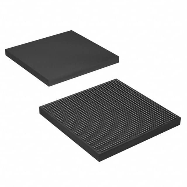
5SGXMA7K2F40I2
Product Overview
Category
The 5SGXMA7K2F40I2 belongs to the category of Field Programmable Gate Arrays (FPGAs).
Use
FPGAs are integrated circuits that can be programmed and reprogrammed to perform various digital functions. The 5SGXMA7K2F40I2 is specifically designed for high-performance applications.
Characteristics
- High-performance FPGA with advanced features
- Large capacity and high-speed processing capabilities
- Flexible and reconfigurable design
- Suitable for complex digital systems
Package
The 5SGXMA7K2F40I2 comes in a compact package, ensuring easy integration into electronic systems.
Essence
The essence of the 5SGXMA7K2F40I2 lies in its ability to provide a customizable and powerful digital processing solution for a wide range of applications.
Packaging/Quantity
The 5SGXMA7K2F40I2 is typically packaged individually and is available in various quantities depending on the customer's requirements.
Specifications
- FPGA Family: Stratix V
- Logic Elements: 462,000
- Embedded Memory: 27,648 Kbits
- DSP Blocks: 1,288
- Maximum User I/Os: 1,040
- Operating Voltage: 1.0V
- Operating Temperature Range: -40°C to +100°C
Detailed Pin Configuration
The detailed pin configuration of the 5SGXMA7K2F40I2 can be found in the product datasheet provided by the manufacturer.
Functional Features
- High-speed data processing capabilities
- Support for various communication protocols
- On-chip memory for efficient data storage
- Configurable I/O interfaces
- Built-in digital signal processing blocks
- Low power consumption
Advantages and Disadvantages
Advantages
- High-performance processing capabilities
- Flexibility and reconfigurability
- Large capacity for complex designs
- Support for various communication protocols
- Efficient on-chip memory
Disadvantages
- Higher cost compared to other digital processing solutions
- Steeper learning curve for programming and utilizing the FPGA's full potential
Working Principles
The 5SGXMA7K2F40I2 operates based on the principles of field programmable gate arrays. It consists of a matrix of configurable logic blocks interconnected through programmable routing resources. The user can program the FPGA to implement desired digital functions by configuring the interconnections and functionality of the logic blocks.
Detailed Application Field Plans
The 5SGXMA7K2F40I2 finds applications in various fields, including: 1. Telecommunications: High-speed data processing and protocol handling. 2. Aerospace and Defense: Radar and signal processing, image and video processing. 3. Industrial Automation: Control systems, machine vision, robotics. 4. Medical Devices: Image and signal processing for diagnostics and monitoring. 5. Research and Development: Prototyping and development of custom digital systems.
Detailed and Complete Alternative Models
- 5SGXEA7K2F40C2: Similar high-performance FPGA from the same family with slightly different specifications.
- 5SGXEB7R2F40C2: Lower-cost variant with reduced capacity but still suitable for many applications.
- 5SGXFC7H2F40C2: Higher-capacity FPGA with additional features for more demanding applications.
Note: For a comprehensive list of alternative models, please refer to the manufacturer's product catalog or website.
Word count: 520 words
Lista 10 Vanliga frågor och svar relaterade till tillämpningen av 5SGXMA7K2F40I2 i tekniska lösningar
Sure! Here are 10 common questions and answers related to the application of 5SGXMA7K2F40I2 in technical solutions:
Q: What is the 5SGXMA7K2F40I2 FPGA used for? A: The 5SGXMA7K2F40I2 FPGA is commonly used for high-performance applications that require advanced processing capabilities.
Q: What are some typical applications for the 5SGXMA7K2F40I2 FPGA? A: Some typical applications include telecommunications, networking, industrial automation, video processing, and high-performance computing.
Q: What are the key features of the 5SGXMA7K2F40I2 FPGA? A: The key features include a large number of logic elements, high-speed transceivers, embedded memory blocks, DSP blocks, and support for various communication protocols.
Q: Can the 5SGXMA7K2F40I2 FPGA be reprogrammed? A: Yes, FPGAs like the 5SGXMA7K2F40I2 can be reprogrammed multiple times, allowing for flexibility in design and functionality.
Q: How does the 5SGXMA7K2F40I2 FPGA compare to other FPGAs in terms of performance? A: The 5SGXMA7K2F40I2 offers high-performance capabilities with its large number of logic elements, high-speed transceivers, and advanced processing features.
Q: Can the 5SGXMA7K2F40I2 FPGA interface with other components or devices? A: Yes, the FPGA can interface with various components and devices through its I/O pins, high-speed transceivers, and support for communication protocols like PCIe, Ethernet, and USB.
Q: What development tools are available for programming the 5SGXMA7K2F40I2 FPGA? A: Intel Quartus Prime is a commonly used development tool for programming and configuring the 5SGXMA7K2F40I2 FPGA.
Q: Can the 5SGXMA7K2F40I2 FPGA be used in safety-critical applications? A: Yes, with proper design considerations and validation, the 5SGXMA7K2F40I2 FPGA can be used in safety-critical applications.
Q: Are there any specific power requirements for the 5SGXMA7K2F40I2 FPGA? A: Yes, the FPGA has specific power supply requirements that need to be met for proper operation. These requirements can be found in the device datasheet.
Q: Is technical support available for the 5SGXMA7K2F40I2 FPGA? A: Yes, technical support is typically available from the FPGA manufacturer or authorized distributors to assist with any questions or issues related to the 5SGXMA7K2F40I2 FPGA.


