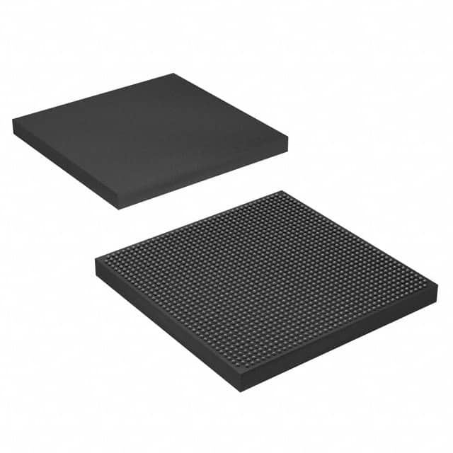
5SGXMA5K2F40I2N
Product Overview
Category
The 5SGXMA5K2F40I2N belongs to the category of Field Programmable Gate Arrays (FPGAs).
Use
FPGAs are integrated circuits that can be programmed and reprogrammed to perform various digital functions. The 5SGXMA5K2F40I2N is specifically designed for high-performance applications.
Characteristics
- High capacity: The 5SGXMA5K2F40I2N offers a large number of logic elements, allowing for complex designs.
- High-speed performance: It operates at high clock frequencies, enabling rapid data processing.
- Versatility: The FPGA can be customized to meet specific application requirements.
- Low power consumption: Despite its high performance, the 5SGXMA5K2F40I2N is designed to minimize power usage.
- Robustness: It is built to withstand harsh operating conditions and maintain reliable performance.
Package and Quantity
The 5SGXMA5K2F40I2N is available in a compact package, typically measuring 40mm x 40mm. It is supplied in tape and reel packaging, with quantities varying based on customer requirements.
Essence
The essence of the 5SGXMA5K2F40I2N lies in its ability to provide flexible and high-performance digital circuitry through programmable logic.
Specifications
- Logic Elements: 5,200,000
- Embedded Memory: 10,000 Kbits
- DSP Blocks: 1,840
- Maximum User I/Os: 1,040
- Transceivers: 96
- Operating Voltage: 1.0V - 1.2V
- Operating Temperature: -40°C to 100°C
Detailed Pin Configuration
The 5SGXMA5K2F40I2N has a complex pin configuration with multiple pins dedicated to various functions. For a detailed pinout diagram and description, please refer to the product datasheet.
Functional Features
- High-speed data processing: The FPGA's architecture allows for efficient parallel processing, enabling rapid execution of complex algorithms.
- Reconfigurability: The 5SGXMA5K2F40I2N can be reprogrammed on-the-fly, allowing for dynamic changes in functionality without requiring hardware modifications.
- Integrated peripherals: It offers a range of built-in peripherals such as memory controllers, Ethernet interfaces, and high-speed serial transceivers, simplifying system integration.
- Error correction: The FPGA includes error correction mechanisms to ensure reliable operation even in the presence of transient faults.
Advantages and Disadvantages
Advantages
- Flexibility: FPGAs offer unparalleled flexibility compared to fixed-function integrated circuits, allowing for customization and adaptation to changing requirements.
- High performance: The 5SGXMA5K2F40I2N delivers exceptional computational power, making it suitable for demanding applications.
- Time-to-market: FPGAs enable rapid prototyping and development cycles, reducing time-to-market for new products.
Disadvantages
- Complexity: Designing and programming FPGAs requires specialized knowledge and expertise.
- Cost: FPGAs tend to be more expensive than off-the-shelf microcontrollers or application-specific integrated circuits (ASICs).
- Power consumption: While efforts have been made to reduce power usage, FPGAs still consume more power compared to dedicated ASICs.
Working Principles
The 5SGXMA5K2F40I2N operates based on the principles of configurable logic. It consists of an array of programmable logic blocks interconnected by configurable routing resources. These logic blocks can be programmed to implement various digital functions, such as arithmetic operations, memory access, and control logic. The configuration of the FPGA is stored in non-volatile memory and can be modified using specialized software tools.
Detailed Application Field Plans
The 5SGXMA5K2F40I2N finds applications in a wide range of fields, including:
- Telecommunications: It is used in high-speed data transmission systems, network routers, and switches.
- Aerospace and Defense: FPGAs are employed in radar systems, avionics, and secure communication equipment.
- Industrial Automation: They are utilized in programmable logic controllers (PLCs), robotics, and machine vision systems.
- Medical Devices: FPGAs play a crucial role in medical imaging, patient monitoring, and diagnostic equipment.
- Automotive: They are integrated into advanced driver-assistance systems (ADAS), infotainment systems, and engine control units (ECUs).
Alternative Models
- 5SGXEA7K2F40C2N
- 5SGXEB6R2F40C2N
- 5
Lista 10 Vanliga frågor och svar relaterade till tillämpningen av 5SGXMA5K2F40I2N i tekniska lösningar
Sure! Here are 10 common questions and answers related to the application of 5SGXMA5K2F40I2N in technical solutions:
Question: What is the purpose of the 5SGXMA5K2F40I2N FPGA?
Answer: The 5SGXMA5K2F40I2N is a Field-Programmable Gate Array (FPGA) designed for high-performance applications that require complex digital logic.Question: What are some typical applications for the 5SGXMA5K2F40I2N?
Answer: This FPGA is commonly used in areas such as telecommunications, aerospace, defense, industrial automation, and high-performance computing.Question: How does the 5SGXMA5K2F40I2N differ from other FPGAs?
Answer: The 5SGXMA5K2F40I2N offers a large number of programmable logic elements, high-speed transceivers, and embedded memory blocks, making it suitable for demanding applications.Question: Can the 5SGXMA5K2F40I2N be used for real-time signal processing?
Answer: Yes, this FPGA is capable of handling real-time signal processing tasks due to its high-speed transceivers and powerful processing capabilities.Question: Is the 5SGXMA5K2F40I2N compatible with industry-standard design tools?
Answer: Yes, this FPGA is supported by popular design software like Quartus Prime, which allows users to program and configure the device easily.Question: Can the 5SGXMA5K2F40I2N be reprogrammed after deployment?
Answer: Yes, FPGAs are known for their reprogrammability, and the 5SGXMA5K2F40I2N can be reconfigured multiple times to adapt to changing requirements.Question: What are the power requirements for the 5SGXMA5K2F40I2N?
Answer: The power requirements vary depending on the specific implementation, but typically, this FPGA requires a supply voltage of around 1.0V to 1.2V.Question: Can the 5SGXMA5K2F40I2N interface with other components or devices?
Answer: Yes, this FPGA supports various communication protocols like PCIe, Ethernet, USB, and DDR3 memory interfaces, enabling seamless integration with other components.Question: Are there any development boards available for the 5SGXMA5K2F40I2N?
Answer: Yes, Intel (formerly Altera) provides development kits specifically designed for this FPGA, which include all the necessary hardware and software tools for prototyping and testing.Question: What kind of technical support is available for the 5SGXMA5K2F40I2N?
Answer: Intel offers comprehensive technical documentation, online forums, and direct customer support to assist users in designing and implementing solutions using the 5SGXMA5K2F40I2N FPGA.


